- 您現(xiàn)在的位置:買賣IC網(wǎng) > PDF目錄373857 > AD1385 (Analog Devices, Inc.) 16-Bit 500 kHz Wide Temperature Range Sampling ADC(16位500kHz寬溫度范圍采樣A/D轉(zhuǎn)換器) PDF資料下載
參數(shù)資料
| 型號(hào): | AD1385 |
| 廠商: | Analog Devices, Inc. |
| 英文描述: | 16-Bit 500 kHz Wide Temperature Range Sampling ADC(16位500kHz寬溫度范圍采樣A/D轉(zhuǎn)換器) |
| 中文描述: | 16位500千赫寬溫采樣ADC(16位500kHz的寬溫度范圍采樣的A / D轉(zhuǎn)換器) |
| 文件頁數(shù): | 11/20頁 |
| 文件大?。?/td> | 360K |
| 代理商: | AD1385 |
AD1385
REV. 0
–11–
mode as long either Hold Command Out or Start Convert is
high. Care is needed in defining system timing to ensure that
the T /H has a minimum of 700 ns for signal acquisition before
another conversion begins. T he minimum width of Start Con-
vert is 20 ns, the sum of t
SCS
and t
SCH
, the minimum setup and
hold times.
T ransmission line effects at the Start Convert and Hold Com-
mand In inputs should be considered when designing circuit
boards for the AD1385. A series termination resistor of 50
to
100
is recommended when the source of either of these sig-
nals is more than a few inches away from the AD1385. T his will
control reflections and transients which could otherwise degrade
the part’s performance.
Output Data
T he output data are multiplexed in two bytes onto an 8-bit data
bus. Data are guaranteed to be stable at the time of the edges of
Data Strobe (Pin 15). Hi/Lo Byte Select (Pin 16) controls
which byte is presented first. If Hi/Lo Byte Select is high, then
BYT E0 is B9–B16 and BYT E1 is B1–B8. T he order of the data
bytes is interchanged when Hi/Lo Byte Select is low. BYT E 0
and BYT E 1 are defined in the timing diagram Figure 17. B1 is
the most significant bit of the reconstructed 16-bit data.
B1 SELECT (Pin 44) determines whether data is presented in
complementary twos complement or complementary offset bi-
nary form. Complementary twos complement data is provided
when B1 Select is LOW.
OE
may be used to place the data bus
into a high impedance state.
T he arithmetic unit in the AD1385 saturates at all 0s or all 1s if
the input range is exceeded.
T able I.
B1 Select
0
1
Complementary T wos Complementary Offset
Complement
7FFFH
FFFFH
8000H
Data Format
–Full-Scale Data
0 V Data
+Full-Scale Data
Binary
FFFFH
8000H
0000H
CALIBRAT ION (Pins 28 and 41)
Calibration corrects for linearity errors in the Reference DAC
arising from internal component mismatches or temperature
changes. It has a negligible effect on gain and offset errors, and
these should be corrected by other means. T he AD1385 must
be calibrated after power-up, and recalibration is recommended
whenever the part’s temperature has changed by more than
15
°
C. Performance degrades gracefully with temperature
changes, resulting in small but gradual decreases in SNR and
increases in distortion which may be eliminated by recalibra-
tion. Calibration codes are stored in internal RAM and are lost
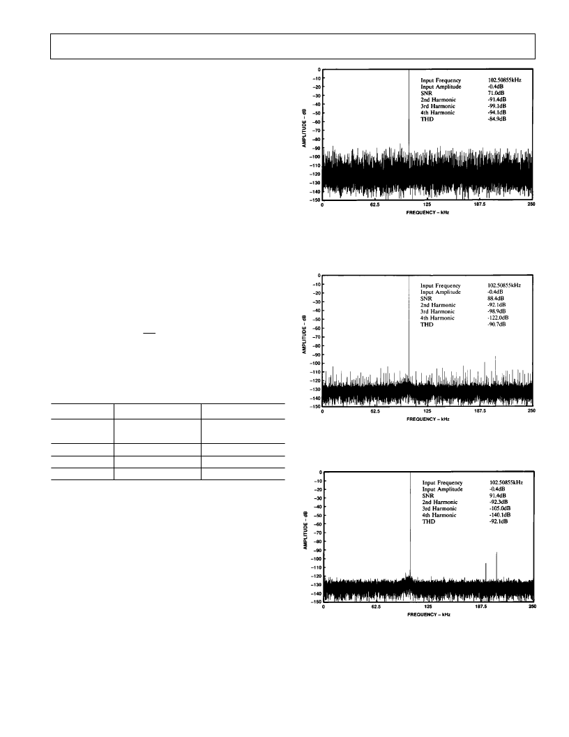
when power is removed. Figures 20–22 show the effects of
uncalibrated versus calibrated operation.
Figure 20. Full-Scale Power Spectral Density after Power-
up at T
CASE
= +25
°
C Without Calibration,
±
5 V Range,
16384-Point FFT, 500 kHz Sample Rate. Compare with
Figure 4.
Figure 21. Full-Scale Power Spectral Density at T
CASE
=
+125
°
C, Calibration Performed at T
CASE
= +25
°
C,
±
5 V
Range, 16384-Point FFT, 500 kHz Sample Rate
Figure 22. Same as Figure 21 Following Recalibration at
T
CASE
= +125
°
C
相關(guān)PDF資料 |
PDF描述 |
|---|---|
| AD1403 | Low Cost, Precision 2.5 V IC References |
| AD1403A | Low Cost, Precision 2.5 V IC References |
| AD1403A* | Low Cost. Precision 2.5 V IC References |
| AD14060BF-4 | Quad-SHARC DSP Multiprocessor Family |
| AD14060 | ECONOLINE: RD & RC - Dual Output from a Single Input Rail- 1kVDC & 2kVDC Isolation- Power Sharing on Output- Custom Solutions Available- UL94V-0 Package Material- Efficiency to 86% |
相關(guān)代理商/技術(shù)參數(shù) |
參數(shù)描述 |
|---|---|
| AD1385KD | 制造商:AD 制造商全稱:Analog Devices 功能描述:16-Bit 500 kHz Wide Temperature Range Sampling ADC |
| AD1385TD | 制造商:Rochester Electronics LLC 功能描述:- Bulk |
| AD1385TD/883B | 制造商:AD 制造商全稱:Analog Devices 功能描述:16-Bit 500 kHz Wide Temperature Range Sampling ADC |
| AD-1386 | 功能描述:烙鐵 CALIBRATION GUAGE RoHS:否 制造商:Weller 產(chǎn)品:Soldering Stations 類型:Digital, Iron, Stand, Cleaner 瓦特:50 W 最大溫度:+ 850 F 電纜類型:US Cord Included |
| AD-1386-CALIBRATION-GA | 制造商:TE Connectivity 功能描述:AD-1386-CALIBRATION-GAUGE 992013-000 |
發(fā)布緊急采購,3分鐘左右您將得到回復(fù)。