- 您現(xiàn)在的位置:買賣IC網(wǎng) > PDF目錄373856 > AD1317KZ (ANALOG DEVICES INC) Ultrahigh Speed Window Comparator with Latch PDF資料下載
參數(shù)資料
| 型號(hào): | AD1317KZ |
| 廠商: | ANALOG DEVICES INC |
| 元件分類: | 運(yùn)動(dòng)控制電子 |
| 英文描述: | Ultrahigh Speed Window Comparator with Latch |
| 中文描述: | COMPARATOR, 10000 uV OFFSET-MAX, CDSO16 |
| 封裝: | GULLWING, HERMETIC SEALED, SMT-16 |
| 文件頁(yè)數(shù): | 3/12頁(yè) |
| 文件大小: | 286K |
| 代理商: | AD1317KZ |
AD1317
–3–
REV. A
ABSOLUTE MAXIMUM RATINGS
1
Power Supply Voltage
+V
S
to GND . . . . . . . . . . . . . . . . . . . . . . . . . . . . . . . +12 V
–V
S
to GND . . . . . . . . . . . . . . . . . . . . . . . . . . . . . . . . . –9 V
Difference from +V
S
to –V
S
. . . . . . . . . . . . . . . . . . . . +16 V
Inputs
VINA/B, VINA, VINB . . . . . . . +V
S
– 13.5 V, –V
S
+ 13.7 V
LEA, LEA, LEB, LEB . . . . . . . . . . +V
S
– 14 V, –V
S
+ 12 V
IE,
IE
. . . . . . . . . . . . . . . . . . . . . .+V
S
– 14 V, –V
S
+ 10.3 V
Outputs
2
QA,
QA
, QB,
QB
. . . . . . . . . . GND – 0.5 V, GND + 3.5 V
Operating Temperature Range . . . . . . . . . . . . . 0
°
C to +70
°
C
Storage Temperature Range
After Soldering . . . . . . . . . . . . . . . . . . . . .–65
°
C to + 125
°
C
Lead Temperature Range (Soldering 20 sec)
3
. . . . . . .+300
°
C
NOTES
1
Stresses above those limits under Absolute Maximum Ratings may cause perma-
nent damage to the device. This is a stress rating only; functional operation of the
device at these or any other conditions above those indicated in the operational
sections of this specification is not implied. Exposure to absolute maximum rating
conditions for extended periods may affect device reliability.
2
Limits apply for shorted output.
3
To ensure lead coplanarity (
±
0.002 inches) and solderability, handling with bare
hands should be avoided and the device should be stored in an environment at
24
°
C
±
5
°
C (75
°
F
±
10
°
F) with relative humidity not to exceed 65%.
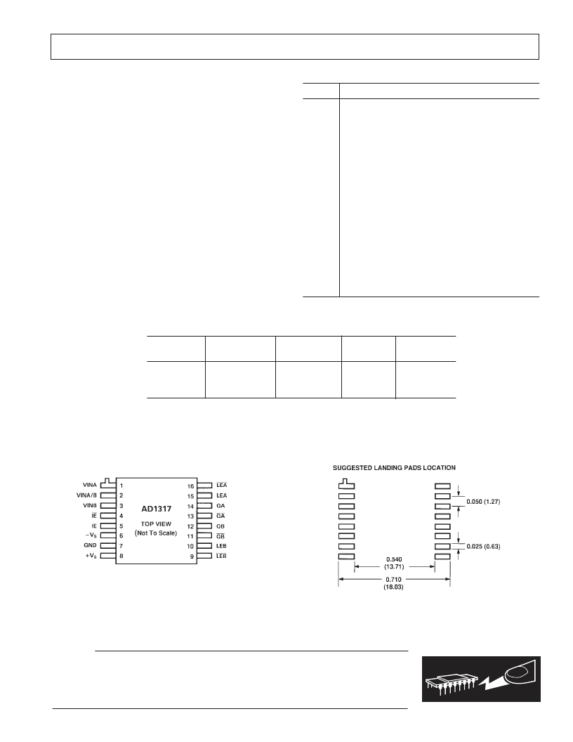
WINDOW COMPARATOR PIN ASSIGNMENT
Pin No.
Description
1
2
3
4
5
6
7
8
9
10
11
12
13
14
15
16
VINA
VINA/B
VINB
IE
IE
–V
S
GND
+V
S
LEB
LEB
QB
QB
QA
QA
LEA
LEA
Noninverting Comparator A Input
Window Comparator Common Input
Inverting Comparator B Input
Input Enable
Input Enable
Negative Supply, –5.2V
Ground
Positive Supply, +10 V
Latch Enable B
Latch Enable B
Comparator B Output
Comparator B Output
Comparator A Output
Comparator A Output
Latch Enable A
Latch Enable A
ORDERING GUIDE
Temperature
Range
Package
Option*
Model
Description
Quantity
AD1317KZ
0
°
C to +70
°
C
16-Lead
Gull Wing
Z-16A
1-24
25–99
100+
*Z = Ceramic Leaded Chip Carrier.
CONNECTION DIAGRAMS
Dimensions shown in inches and (mm).
WARNING!
ESD SENSITIVE DEVICE
CAUTION
ESD (electrostatic discharge) sensitive device. Electrostatic charges as high as 4000 V readily
accumulate on the human body and test equipment and can discharge without detection.
Although the AD1317 features proprietary ESD protection circuitry, permanent damage may
occur on devices subjected to high energy electrostatic discharges. Therefore, proper ESD
precautions are recommended to avoid performance degradation or loss of functionality.
相關(guān)PDF資料 |
PDF描述 |
|---|---|
| AD1324KZ | Ultrahigh Speed Pin Driver with Inhibit Mode |
| AD1324 | Ultrahigh Speed Pin Driver with Inhibit Mode |
| AD13280 | ECONOLINE: RD & RC - Dual Output from a Single Input Rail- 1kVDC & 2kVDC Isolation- Power Sharing on Output- Custom Solutions Available- UL94V-0 Package Material- Efficiency to 86% |
| AD13280AF | Dual Channel, 12-Bit, 80 MSPS A/D Converter with Analog Input Signal Conditioning |
| AD13280AZ | Dual Channel, 12-Bit, 80 MSPS A/D Converter with Analog Input Signal Conditioning |
相關(guān)代理商/技術(shù)參數(shù) |
參數(shù)描述 |
|---|---|
| AD-1319-10 | 制造商:TE Connectivity 功能描述: |
| AD-1319-12-HOLDNG-FIXT | 制造商:TE Connectivity 功能描述:018579-000 |
| AD-1319-12-HOLDNG-FIXTURE | 制造商:TE Connectivity 功能描述:AD-1319-12-HOLDNG-FIXTURE |
| AD-1319-9 | 制造商:TE Connectivity 功能描述:AD-1319-9 制造商:TE Connectivity 功能描述:5-1197687-0,993850-000 AD-1319-9-HOLD-FIX-PACKAG |
| AD-1319-9-HOLD-FIX-PACKAG | 制造商:TE Connectivity 功能描述:AD-1319-9 |
發(fā)布緊急采購(gòu),3分鐘左右您將得到回復(fù)。