- 您現(xiàn)在的位置:買賣IC網(wǎng) > PDF目錄373856 > AD12400JWS (ANALOG DEVICES INC) 12-Bit 400 MSPS A/D Converter PDF資料下載
參數(shù)資料
| 型號: | AD12400JWS |
| 廠商: | ANALOG DEVICES INC |
| 元件分類: | ADC |
| 英文描述: | 12-Bit 400 MSPS A/D Converter |
| 中文描述: | 1-CH 12-BIT PROPRIETARY METHOD ADC, PARALLEL ACCESS |
| 封裝: | 2.9 X 2.6 INCH, 0.6 INCH HEIGHT, MODULE |
| 文件頁數(shù): | 16/28頁 |
| 文件大小: | 403K |
| 代理商: | AD12400JWS |
第1頁第2頁第3頁第4頁第5頁第6頁第7頁第8頁第9頁第10頁第11頁第12頁第13頁第14頁第15頁當(dāng)前第16頁第17頁第18頁第19頁第20頁第21頁第22頁第23頁第24頁第25頁第26頁第27頁第28頁
AD12400
Rev. 0 | Page 16 of 28
ANALOG INPUT
The AD12400 analog input is ac-coupled using a proprietary,
transformer front end circuit that provides 1 dB of gain flatness
over the first Nyquist zone and a –3 dB bandwidth of 450 MHz.
This front end circuit provides a VSWR of 1.5 (50 Ω) over the
first Nyquist zone, and the typical full-scale input is 3.2 V p-p
The MiniCircuits HELA-10 amplifier module can be used to
drive the input at these power levels.
CLOCK INPUT
The AD12400 requires a 400 MSPS encode that is divided by 2
and distributed to each ADC channel, 180° out of phase from
each other. Internal ac-coupling and bias networks provide the
framework for flexible clock input requirements that include
single-ended sine-wave, single-ended PECL, and differential
PECL. While the AD12400 is tested and calibrated using a
single-ended sine-wave, properly designed PECL circuits that
provide fast slew rates (>1V/ns) and minimize ringing will
result in comparable dynamic range performance.
There are two major factors to consider when designing the
input clock circuit for the AD12400: aperture jitter and
harmonic content. The relationship between aperture jitter and
SNR can be characterized using the following equation. The
equation assumes a single-tone full-scale input signal.
(
)
)
(LSB
noise
input
ADC
(LSB)
DNL
=
ADC
(bits)
resolution
ADC
jitter
Aperture
frequency
Input
=
2
2
2
2
2
2
1
5
1
2
0
2
log
20
rms
NOISE
V
N
ε
JRMS
=
t
A
f
N
V
N
t
f
SNR
NOISErms
JRMS
A
=
=
×
+
ε
+
×
+
×
×
π
=
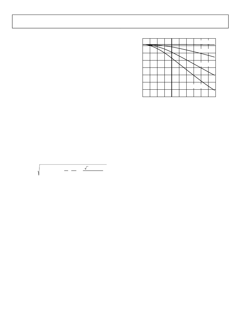
Figure 20 displays the application of this relationship to full-
scale, single-tone input signal on the AD12400, where the DNL
was assumed to be 0.4 LSB, and the input noise was assumed to
be 0.8 LSBrms. The vertical marker at 0.4 ps displays the SNR at
the jitter level present in the AD12400 evaluation system,
including the jitter associated with the AD12400 itself.
57
58
59
60
61
62
63
64
65
0
0
0.1
0.2
0.3
APERTURE JITTER (ps rms)
0.4
0.5
0.6
0.7
0.8
0.9
1.0
S
A
IN
= 10MHz
A
IN
= 65MHz
A
IN
= 128MHz
A
IN
= 180MHz
Figure 20. SNR vs. Aperture Jitter
In addition to jitter, the harmonic content of single-ended sine
wave clock sources must be controlled as well. The clock source
used in the test and calibration process has a harmonic
performance that is better than 60 dBc. Also, when using PECL
or other square-wave clock sources, unstable behavior such as
overshoot and ringing can affect phase matching and degrade
the image spur performance
DIGITAL OUTPUTS
The AD12400’s digital post processing circuit provides two
parallel, 12-bit 200 MSPS data output buses. By providing two
output busses that operate at one half the conversion rate, the
AD12400 eliminates the need for large, expensive, high power
demultiplexing circuits. The output data format is twos
complement, maintaining the standard set by other high speed
A/D converters such as the AD9430 and AD6645. Data-ready
signals are provided for facilitating proper timing in the data
capture circuit. Finally, the digital post processing circuit can be
configured to provide alternate data output formats. Contact the
factory for more details.
POWER SUPPLIES
The AD12400 requires three different supply voltages: a 1.5 V
supply for the digital post processing circuit, a 3.3 V supply to
facilitate digital I/O through the system, and a 3.8 V supply for
the analog conversion and clock distribution circuits. The
AD12400 incorporates two key features that result in solid
power supply rejection ratio (PSRR) performance. First, on-
board linear regulators are used to provide an extra level of
power supply rejection for the analog circuits. The linear
regulator used to supply the A/D converters provides an
additional 60 dB of rejection at 100 kHz. Second, in order to
address higher frequency noise (where the linear regulators’
rejection degrades), the AD12400 incorporates high quality
ceramic decoupling capacitors.
相關(guān)PDF資料 |
PDF描述 |
|---|---|
| AD12400KWS | 12-Bit 400 MSPS A/D Converter |
| AD1315KZ | High Speed Active Load with Inhibit Mode |
| AD1315 | High Speed Active Load with Inhibit Mode |
| AD1317 | Ultrahigh Speed Window Comparator with Latch |
| AD1317KZ | Ultrahigh Speed Window Comparator with Latch |
相關(guān)代理商/技術(shù)參數(shù) |
參數(shù)描述 |
|---|---|
| AD12400KWS | 制造商:Analog Devices 功能描述:ADC Dual 400Msps 12-bit Parallel/LVDS |
| AD12401 | 制造商:AD 制造商全稱:Analog Devices 功能描述:12-Bit, 400 MSPS A/D Converter |
| AD12401/KIT | 制造商:AD 制造商全稱:Analog Devices 功能描述:12-Bit, 400 MSPS A/D Converter |
| AD12401-326JWS | 制造商:AD 制造商全稱:Analog Devices 功能描述:12-Bit, 400 MSPS A/D Converter |
| AD12401-326KWS | 制造商:Analog Devices 功能描述:ADC Dual 326Msps 12-bit Parallel 120-Pin SMD |
發(fā)布緊急采購,3分鐘左右您將得到回復(fù)。