- 您現(xiàn)在的位置:買賣IC網(wǎng) > PDF目錄362053 > ACH16245DGG (NXP SEMICONDUCTORS) JT 55C 55#22D PIN PLUG PDF資料下載
參數(shù)資料
| 型號: | ACH16245DGG |
| 廠商: | NXP SEMICONDUCTORS |
| 元件分類: | 通用總線功能 |
| 英文描述: | JT 55C 55#22D PIN PLUG |
| 中文描述: | ALVC/VCX/A SERIES, DUAL 8-BIT TRANSCEIVER, TRUE OUTPUT, PDSO48 |
| 文件頁數(shù): | 2/10頁 |
| 文件大?。?/td> | 91K |
| 代理商: | ACH16245DGG |
Philips Semiconductors
Product specification
74ALVC16245/
74ALVCH16245
16-bit bus transceiver with direction pin (3-State)
2
1998 Jun 29
853-2083 19638
FEATURES
Wide supply voltage range of 1.2V to 3.6V
Complies with JEDEC standard no. 8-1A
CMOS low power consumption
MULTIBYTE
TM
flow-through standard pin-out architecture
Low inductance multiple V
CC
and ground pins for minimum noise
and ground bounce
Direct interface with TTL levels
All data inputs have bus hold (74ALVCH16245 only)
Output drive capability 50
transmission lines @ 85
°
C
Current drive
±
24 mA at 3.0 V
DESCRIPTION
The 74ALVC16245(74ALVCH16245) is a 16-bit transceiver featuring
non-inverting 3-State bus compatible outputs in both send and
receive directions.
The 74ALVC16245(74ALVCH16245) features two output enable
(nOE) inputs for easy cascading and two send/receive (nDIR) inputs
for direction control. nOE controls the outputs so that the buses are
effectively isolated. This device can be used as two 8-bit
transceivers or one 16-bit transceiver.
The 74ALVCH16245 has active bus hold circuitry which is provided
to hold unused or floating data inputs at a valid logic level. This
feature eliminates the need for external pull-up or pull-down
resistors.
The 74ALVC16245 has 5V tolerant inputs.
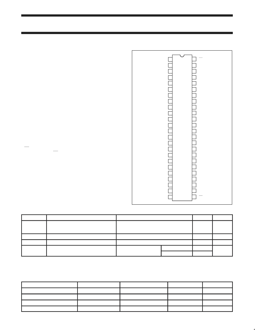
PIN CONFIGURATION
1
2
3
4
5
6
7
8
9
10
11
12
13
14
15
16
17
18
19
20
29
30
31
32
33
34
35
36
37
38
39
40
41
42
43
44
45
46
47
48
GND
V
CC1
GND
GND
V
CC1
2A5
2A4
V
CC2
2A3
2A2
GND
2A1
2A0
1A7
1A6
GND
1A5
1A4
V
CC2
1A3
1A2
GND
1A1
1A0
1OE
21
22
23
24
25
26
27
28
GND
2DIR
2OE
2A7
2A6
GND
SW00198
1DIR
1B0
1B1
1B2
1B3
1B4
1B5
1B6
1B7
2B0
2B1
2B2
2B3
2B4
2B5
2B6
2B7
QUICK REFERENCE DATA
GND = 0V; T
amb
= 25
°
C; t
r
= t
f
≤
2.5ns
SYMBOL
PARAMETER
CONDITIONS
TYPICAL
UNIT
t
PHL
/t
PLH
Propagation delay
An to Bn;
Bn to An
V
CC
= 2.5V, CL = 30pF
V
CC
= 3.3V, CL = 50pF
1.9
ns
C
I
C
I/O
Input capacitance
4.0
pF
Input/output capacitance
8.0
pF
C
PD
Power dissipation capacitance per buffer
V = GND to V
CC1
Outputs enabled
29
pF
Outputs disabled
5
NOTE:
1. C
PD
is used to determine the dynamic power dissipation (P
D
in
μ
W):
P
D
= C
PD
×
V
CC2
×
f
i
+ (C
L
×
V
CC2
×
f
o
) where: f
i
= input frequency in MHz; C
L
= output load capacitance in pF;
f
o
= output frequency in MHz; V
CC
= supply voltage in V; (C
L
×
V
CC2
×
f
o
) = sum of the outputs.
ORDERING INFORMATION
PACKAGES
TEMPERATURE RANGE
OUTSIDE NORTH AMERICA
NORTH AMERICA
DWG NUMBER
48-Pin Plastic SSOP Type III
–40
°
C to +85
°
C
–40
°
C to +85
°
C
–40
°
C to +85
°
C
–40
°
C to +85
°
C
74ALVC16245 DL
AC16245 DL
SOT370-1
48-Pin Plastic TSSOP Type II
74ALVC16245 DGG
AC16245 DGG
SOT362-1
48-Pin Plastic SSOP Type III
74ALVCH16245 DL
ACH16245 DL
SOT370-1
48-Pin Plastic TSSOP Type II
74ALVCH16245 DGG
ACH16245 DGG
SOT362-1
相關(guān)PDF資料 |
PDF描述 |
|---|---|
| ACH16245DL | 2.5V/3.3V 16-bit bus transceiver with direction pin 3-State |
| AC162834ADGG | 18-bit registered driver with inverted register enable and 30ohm termination resistors 3-State |
| AC164010 | SOCKELMODUL |
| AC164012 | SOCKELMODUL |
| AC164026 | SOCKET MODULE SOIC/TSSOP |
相關(guān)代理商/技術(shù)參數(shù) |
參數(shù)描述 |
|---|---|
| ACH16245DL | 制造商:PHILIPS 制造商全稱:NXP Semiconductors 功能描述:2.5V/3.3V 16-bit bus transceiver with direction pin 3-State |
| ACH162827DGG | 制造商:PHILIPS 制造商全稱:NXP Semiconductors 功能描述:20-bit buffer/line driver, non-inverting,with 30ohm termination resistors (3-State) |
| ACH16373DGG | 制造商:PHILIPS 制造商全稱:NXP Semiconductors 功能描述:2.5V/3.3V 16-bit D-type transparent latch 3-State |
| ACH16373DL | 制造商:PHILIPS 制造商全稱:NXP Semiconductors 功能描述:2.5V/3.3V 16-bit D-type transparent latch 3-State |
| ACH16374DGG | 制造商:PHILIPS 制造商全稱:NXP Semiconductors 功能描述:2.5V/3.3V 16-bit edge-triggered D-type flip-flop 3-State |
發(fā)布緊急采購,3分鐘左右您將得到回復(fù)。