- 您現(xiàn)在的位置:買賣IC網(wǎng) > PDF目錄352476 > A42MX16-1PQ100A (Electronic Theatre Controls, Inc.) 40MX and 42MX FPGA Families PDF資料下載
參數(shù)資料
| 型號: | A42MX16-1PQ100A |
| 廠商: | Electronic Theatre Controls, Inc. |
| 英文描述: | 40MX and 42MX FPGA Families |
| 中文描述: | 40MX和42MX FPGA系列 |
| 文件頁數(shù): | 119/120頁 |
| 文件大?。?/td> | 854K |
| 代理商: | A42MX16-1PQ100A |
第1頁第2頁第3頁第4頁第5頁第6頁第7頁第8頁第9頁第10頁第11頁第12頁第13頁第14頁第15頁第16頁第17頁第18頁第19頁第20頁第21頁第22頁第23頁第24頁第25頁第26頁第27頁第28頁第29頁第30頁第31頁第32頁第33頁第34頁第35頁第36頁第37頁第38頁第39頁第40頁第41頁第42頁第43頁第44頁第45頁第46頁第47頁第48頁第49頁第50頁第51頁第52頁第53頁第54頁第55頁第56頁第57頁第58頁第59頁第60頁第61頁第62頁第63頁第64頁第65頁第66頁第67頁第68頁第69頁第70頁第71頁第72頁第73頁第74頁第75頁第76頁第77頁第78頁第79頁第80頁第81頁第82頁第83頁第84頁第85頁第86頁第87頁第88頁第89頁第90頁第91頁第92頁第93頁第94頁第95頁第96頁第97頁第98頁第99頁第100頁第101頁第102頁第103頁第104頁第105頁第106頁第107頁第108頁第109頁第110頁第111頁第112頁第113頁第114頁第115頁第116頁第117頁第118頁當(dāng)前第119頁第120頁
98
4958B–AUTO–11/10
Atmel ATA6285/ATA6286 [Preliminary]
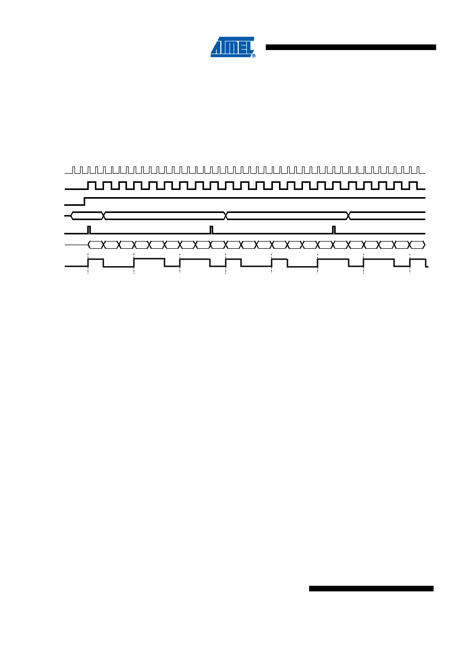
3.13.6.7
Mode 7: Modulator Mode with SSI and Modulator Output T2O2 at the PD6 Pin
The Timer2/Counter2 can be supplied with internal/external clocks. Mode 7 uses only one mod-
ulator I/O pin (SO --> T2O2). The port pins (PD5, PD7) can be used as general digital I/O. The
timer output clock (CLK
T2) can be used to supply the SSI with shift clock. Together with the con-
tinuous serial data stream generated by Synchronous Serial Interface (SSI) the modulator mode
7 of the timer allows the generation of Biphase code, Manchester code or PWM code. Figure
3-43 shows an example of PWM code generation.
Figure 3-43. Modulator Mode and Modulator Output at the T2O2 Pin, Timing Diagram
PWM Code:
Standard practice dictates a 2/3, 1/3 format (of the overall bit period).
Each bit comprise High and a Low in a 2/3, 1/3 - partition.
In the same moment the 8-bit Shift register (SR) is loaded with the T2MDR (TXD) data the first
bit (MSB) will appear at T202 output pin
3.13.6.8
Mode 8/9: Transmit Mode with SSI and Modulator Outputs T2O1/T2O2 at the PD5/PD6 Pins
The Timer2/Counter2 can be supplied with internal/external clocks. Mode 8/9 uses two modula-
tor I/O pins (SO --> T2O1 and SCLK --> T2O2 in mode 8 and SCLK --> T2O1 and SO --> T2O2
in mode 9). The port pin PD7 can be used as general digital I/O. The timer output clock (CLK
T2)
can be used to supply the SSI with a shift clock. The transmit mode of the timer allows a SSI
synchronous data transfer between the ATA6289 and peripheral devices. The data is always
shifted from Master (SSI) to Slave on the Serial data Output line (SO), synchronized to either the
rising or falling edge of the shift clock output line (SCLK). Serial data is organized in 8-bit tele-
grams which are shifted with the most significant bit (MSB) first to the serial data output line
(SO). The Figure 3-44 on page 99 shows an example of a synchronous serial data transmission.
0xB4
0x49
0x9B
T2MDR
(TXD)
PMW coded
bit stream
Load 8-bit Shift
Register (SR)
T2SSIE
Shifted Value of 8-bit
Shift Register (SR)
T202
SCLK
CLKT2
Bit 3 = ’1’
Bit 2 = ’0’
Bit 4 = ’1’
Bit 6 = ’0’
Bit 7 = ’1’
Bit 5 = ’0’
Bit 1 = ’0’
Bit 0 = ’1’
0xB0
0xD8
0x6C
0x36
0x9B
0x68
0x80
0x40
0xD0
0xA0
0xB4
0x80
0x24
0x40
0x20
0x48
0x90
0x60
0x92
0x49
0xC0
0x80
相關(guān)PDF資料 |
PDF描述 |
|---|---|
| A42MX24-1PQ100A | TRANSF 4000 OHM PRI. 0MA DC TEL |
| A42MX02-1PQ100B | Line Matching Transformer; Current Rating:0A; Insertion Loss:1dB; Leaded Process Compatible:Yes; Peak Reflow Compatible (260 C):Yes; Size:0.89 x 0.812 x 0.715 in; Terminal Type:PCB Thru Hole RoHS Compliant: Yes |
| A42MX04-1PQ100B | TRANSF 600 OHM 100MA DC TEL |
| A42MX09-1PQ100B | TRANSF 600 SPLIT PRI .75MA DC TE |
| A42MX16-1PQ100B | TRANSF 600 OHM 0MA DC TEL |
相關(guān)代理商/技術(shù)參數(shù) |
參數(shù)描述 |
|---|---|
| A42MX16-1PQ100B | 制造商:未知廠家 制造商全稱:未知廠家 功能描述:40MX and 42MX FPGA Families |
| A42MX16-1PQ100ES | 制造商:ACTEL 制造商全稱:Actel Corporation 功能描述:40MX and 42MX FPGA Families |
| A42MX16-1PQ100I | 功能描述:IC FPGA MX SGL CHIP 24K 100-PQFP RoHS:否 類別:集成電路 (IC) >> 嵌入式 - FPGA(現(xiàn)場可編程門陣列) 系列:MX 標(biāo)準(zhǔn)包裝:40 系列:SX-A LAB/CLB數(shù):6036 邏輯元件/單元數(shù):- RAM 位總計(jì):- 輸入/輸出數(shù):360 門數(shù):108000 電源電壓:2.25 V ~ 5.25 V 安裝類型:表面貼裝 工作溫度:0°C ~ 70°C 封裝/外殼:484-BGA 供應(yīng)商設(shè)備封裝:484-FPBGA(27X27) |
| A42MX16-1PQ100M | 制造商:Microsemi Corporation 功能描述:FPGA 24K GATES 608 CELLS 119MHZ/198MHZ 0.45UM 3.3V/5V 100PQF - Trays 制造商:Microsemi Corporation 功能描述:IC FPGA 83 I/O 100PQFP 制造商:Microsemi Corporation 功能描述:IC FPGA MX SGL CHIP 24K 100-PQFP |
| A42MX16-1PQ160 | 功能描述:IC FPGA MX SGL CHIP 24K 160-PQFP RoHS:否 類別:集成電路 (IC) >> 嵌入式 - FPGA(現(xiàn)場可編程門陣列) 系列:MX 標(biāo)準(zhǔn)包裝:40 系列:SX-A LAB/CLB數(shù):6036 邏輯元件/單元數(shù):- RAM 位總計(jì):- 輸入/輸出數(shù):360 門數(shù):108000 電源電壓:2.25 V ~ 5.25 V 安裝類型:表面貼裝 工作溫度:0°C ~ 70°C 封裝/外殼:484-BGA 供應(yīng)商設(shè)備封裝:484-FPBGA(27X27) |
發(fā)布緊急采購,3分鐘左右您將得到回復(fù)。