- 您現(xiàn)在的位置:買賣IC網(wǎng) > PDF目錄362022 > A42MX09-FPQ160 Field Programmable Gate Array (FPGA) PDF資料下載
參數(shù)資料
| 型號(hào): | A42MX09-FPQ160 |
| 英文描述: | Field Programmable Gate Array (FPGA) |
| 中文描述: | 現(xiàn)場(chǎng)可編程門陣列(FPGA) |
| 文件頁(yè)數(shù): | 8/116頁(yè) |
| 文件大?。?/td> | 3110K |
| 代理商: | A42MX09-FPQ160 |
第1頁(yè)第2頁(yè)第3頁(yè)第4頁(yè)第5頁(yè)第6頁(yè)第7頁(yè)當(dāng)前第8頁(yè)第9頁(yè)第10頁(yè)第11頁(yè)第12頁(yè)第13頁(yè)第14頁(yè)第15頁(yè)第16頁(yè)第17頁(yè)第18頁(yè)第19頁(yè)第20頁(yè)第21頁(yè)第22頁(yè)第23頁(yè)第24頁(yè)第25頁(yè)第26頁(yè)第27頁(yè)第28頁(yè)第29頁(yè)第30頁(yè)第31頁(yè)第32頁(yè)第33頁(yè)第34頁(yè)第35頁(yè)第36頁(yè)第37頁(yè)第38頁(yè)第39頁(yè)第40頁(yè)第41頁(yè)第42頁(yè)第43頁(yè)第44頁(yè)第45頁(yè)第46頁(yè)第47頁(yè)第48頁(yè)第49頁(yè)第50頁(yè)第51頁(yè)第52頁(yè)第53頁(yè)第54頁(yè)第55頁(yè)第56頁(yè)第57頁(yè)第58頁(yè)第59頁(yè)第60頁(yè)第61頁(yè)第62頁(yè)第63頁(yè)第64頁(yè)第65頁(yè)第66頁(yè)第67頁(yè)第68頁(yè)第69頁(yè)第70頁(yè)第71頁(yè)第72頁(yè)第73頁(yè)第74頁(yè)第75頁(yè)第76頁(yè)第77頁(yè)第78頁(yè)第79頁(yè)第80頁(yè)第81頁(yè)第82頁(yè)第83頁(yè)第84頁(yè)第85頁(yè)第86頁(yè)第87頁(yè)第88頁(yè)第89頁(yè)第90頁(yè)第91頁(yè)第92頁(yè)第93頁(yè)第94頁(yè)第95頁(yè)第96頁(yè)第97頁(yè)第98頁(yè)第99頁(yè)第100頁(yè)第101頁(yè)第102頁(yè)第103頁(yè)第104頁(yè)第105頁(yè)第106頁(yè)第107頁(yè)第108頁(yè)第109頁(yè)第110頁(yè)第111頁(yè)第112頁(yè)第113頁(yè)第114頁(yè)第115頁(yè)第116頁(yè)
40MX and 42MX FPGA Families
8
v5.0
MultiPlex I/O Modules
MultiPlex I/O supports the most common voltage standards
today: pure 5.0V operation, pure 3.3V operation, and mixed
3.3V operation with 5.0V I/O tolerance for maximum
performance. Internal array performance is retained in 3.3V
systems by using complimentary pass gates that operate as
fast as they do at 5.0V at 3.3V.
MultiPlex I/O includes selectable PCI output drives in
certain 42MX devices, enabling 100% PCI-compliance for
both 5.0V and 3.3V systems. For low-power systems,
MultiPlex I/O is used to turn off all inputs and outputs to cut
current consumption to below 100μA.
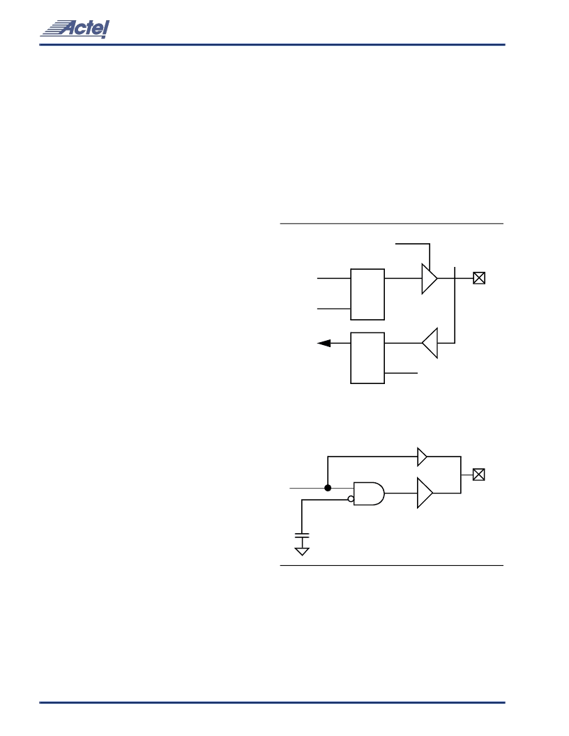
The MultiPlex I/O modules provide the interface between
the device pins and the logic array. The top of
Figure 6
is a
block diagram of the 42MX I/O module. A variety of user
functions, determined by a library macro selection, can be
implemented in the module. (Refer to the
Macro Library
Guide
for more information.) All 42MX I/O modules contain
tristate buffers, with input and output latches that can be
configured for input, output, or bi-directional operation.
All 42MX devices contain flexible I/O structures (
Figure 7 on
page 9
), where each output pin has a dedicated
output-enable control. The I/O module can be used to latch
input or output data, or both, providing a fast set-up time. In
addition, the Actel Designer Series software tools can build
a D-type flip-flop using a C-module to register input and
output signals. To achieve 5.0V or 3.3V PCI-compliant output
drives on A42MX24 and A42MX36 devices, a chip-wide PCI
fuse is programmed. When the PCI fuse is not programmed,
the output drive is standard. (See the bottom portion of
Figure 6
.)
Actel
’
s Designer Series development tools provide a design
library of I/O macrofunctions that can implement all I/O
configurations supported by the MX FPGAs.
Routing Structure
The MX architecture uses vertical and horizontal routing
tracks to interconnect the various logic and I/O modules.
These routing tracks are metal interconnects that may be
either of continuous length or broken into pieces called
segments. Varying segment lengths allows the interconnect
of over 90% of design tracks to occur with only two antifuse
connections. Segments can be joined together at the ends
using antifuses to increase their lengths up to the full length
of the track. All interconnects can be accomplished with a
maximum of four antifuses.
Horizontal Routing
Horizontal channels are located between the rows of
modules and are composed of several routing tracks. The
horizontal routing tracks within the channel are divided
into one or more segments. The minimum horizontal
segment length is the width of a module pair, and the
maximum horizontal segment length is the full length of the
channel. Any segment that spans more than one-third at the
row length is considered a long horizontal segment. A
typical channel is shown in
Figure 8 on page 9
.
Non-dedicated horizontal routing tracks are used to route
signal nets; dedicated routing tracks are used for global
clock networks and for power and ground tie-off tracks.
Vertical Routing
Another set of routing tracks run vertically through the
module. There are three types of vertical tracks: input,
output, and long, which are also divided into one or more
segments. Each segment in an input track is dedicated to
the input of a particular module; each segment in an output
track is dedicated to the output of a particular module. Long
segments are uncommitted and can be assigned during
Figure 6
42MX I/O Module
G/CLK*
Q
D
EN
PAD
* Can be Configured as a Latch or D Flip-Flop
(Using C-Module)
From Array
To Array
G/CLK*
Q
D
Signal
PCI Enable
Fuse
PCI
Drive
Schematic
STD
Output
相關(guān)PDF資料 |
PDF描述 |
|---|---|
| A42MX09-FPQ160I | Field Programmable Gate Array (FPGA) |
| A42MX09-FPQ160M | Field Programmable Gate Array (FPGA) |
| A42MX09-FTQ176 | Field Programmable Gate Array (FPGA) |
| A42MX09-FTQ176I | Field Programmable Gate Array (FPGA) |
| A42MX09-FTQ176M | Field Programmable Gate Array (FPGA) |
相關(guān)代理商/技術(shù)參數(shù) |
參數(shù)描述 |
|---|---|
| A42MX09-FPQ160I | 制造商:未知廠家 制造商全稱:未知廠家 功能描述:Field Programmable Gate Array (FPGA) |
| A42MX09-FPQ160M | 制造商:未知廠家 制造商全稱:未知廠家 功能描述:Field Programmable Gate Array (FPGA) |
| A42MX09-FPQG100 | 功能描述:IC FPGA MX SGL CHIP 14K 100-PQFP RoHS:是 類別:集成電路 (IC) >> 嵌入式 - FPGA(現(xiàn)場(chǎng)可編程門陣列) 系列:MX 標(biāo)準(zhǔn)包裝:90 系列:ProASIC3 LAB/CLB數(shù):- 邏輯元件/單元數(shù):- RAM 位總計(jì):36864 輸入/輸出數(shù):157 門數(shù):250000 電源電壓:1.425 V ~ 1.575 V 安裝類型:表面貼裝 工作溫度:-40°C ~ 125°C 封裝/外殼:256-LBGA 供應(yīng)商設(shè)備封裝:256-FPBGA(17x17) |
| A42MX09-FPQG160 | 功能描述:IC FPGA MX SGL CHIP 14K 160-PQFP RoHS:是 類別:集成電路 (IC) >> 嵌入式 - FPGA(現(xiàn)場(chǎng)可編程門陣列) 系列:MX 標(biāo)準(zhǔn)包裝:90 系列:ProASIC3 LAB/CLB數(shù):- 邏輯元件/單元數(shù):- RAM 位總計(jì):36864 輸入/輸出數(shù):157 門數(shù):250000 電源電壓:1.425 V ~ 1.575 V 安裝類型:表面貼裝 工作溫度:-40°C ~ 125°C 封裝/外殼:256-LBGA 供應(yīng)商設(shè)備封裝:256-FPBGA(17x17) |
| A42MX09-FTQ100 | 制造商:未知廠家 制造商全稱:未知廠家 功能描述:40MX and 42MX FPGA Families |
發(fā)布緊急采購(gòu),3分鐘左右您將得到回復(fù)。