- 您現(xiàn)在的位置:買賣IC網(wǎng) > PDF目錄362022 > A40MX04-3PQ100 Field Programmable Gate Array (FPGA) PDF資料下載
參數(shù)資料
| 型號(hào): | A40MX04-3PQ100 |
| 英文描述: | Field Programmable Gate Array (FPGA) |
| 中文描述: | 現(xiàn)場(chǎng)可編程門陣列(FPGA) |
| 文件頁(yè)數(shù): | 10/116頁(yè) |
| 文件大小: | 3110K |
| 代理商: | A40MX04-3PQ100 |
第1頁(yè)第2頁(yè)第3頁(yè)第4頁(yè)第5頁(yè)第6頁(yè)第7頁(yè)第8頁(yè)第9頁(yè)當(dāng)前第10頁(yè)第11頁(yè)第12頁(yè)第13頁(yè)第14頁(yè)第15頁(yè)第16頁(yè)第17頁(yè)第18頁(yè)第19頁(yè)第20頁(yè)第21頁(yè)第22頁(yè)第23頁(yè)第24頁(yè)第25頁(yè)第26頁(yè)第27頁(yè)第28頁(yè)第29頁(yè)第30頁(yè)第31頁(yè)第32頁(yè)第33頁(yè)第34頁(yè)第35頁(yè)第36頁(yè)第37頁(yè)第38頁(yè)第39頁(yè)第40頁(yè)第41頁(yè)第42頁(yè)第43頁(yè)第44頁(yè)第45頁(yè)第46頁(yè)第47頁(yè)第48頁(yè)第49頁(yè)第50頁(yè)第51頁(yè)第52頁(yè)第53頁(yè)第54頁(yè)第55頁(yè)第56頁(yè)第57頁(yè)第58頁(yè)第59頁(yè)第60頁(yè)第61頁(yè)第62頁(yè)第63頁(yè)第64頁(yè)第65頁(yè)第66頁(yè)第67頁(yè)第68頁(yè)第69頁(yè)第70頁(yè)第71頁(yè)第72頁(yè)第73頁(yè)第74頁(yè)第75頁(yè)第76頁(yè)第77頁(yè)第78頁(yè)第79頁(yè)第80頁(yè)第81頁(yè)第82頁(yè)第83頁(yè)第84頁(yè)第85頁(yè)第86頁(yè)第87頁(yè)第88頁(yè)第89頁(yè)第90頁(yè)第91頁(yè)第92頁(yè)第93頁(yè)第94頁(yè)第95頁(yè)第96頁(yè)第97頁(yè)第98頁(yè)第99頁(yè)第100頁(yè)第101頁(yè)第102頁(yè)第103頁(yè)第104頁(yè)第105頁(yè)第106頁(yè)第107頁(yè)第108頁(yè)第109頁(yè)第110頁(yè)第111頁(yè)第112頁(yè)第113頁(yè)第114頁(yè)第115頁(yè)第116頁(yè)
40MX and 42MX FPGA Families
10
v5.0
Test Circuitry
All devices contain Actel
’
s ActionProbe test circuitry which
test and debug a design once it is programmed into a device.
Once a device has been programmed, the ActionProbe test
circuitry allows the designer to probe any internal node
during device operation to aid in debugging a design. In
addition, 42MX devices contain IEEE Standard 1149.1
boundary scan test circuitry.
IEEE Standard 1149.1 Boundary Scan Testing (BST)
IEEE Standard 1149.1 defines a four-pin Test Access Port
(TAP) interface for testing integrated circuits in a system.
The 42MX family provides five BST pins: Test Data In (TDI),
Test Data Out (TDO), Test Clock (TCK), and Test Mode
Select Test Reset (TRST) (42MX24A only). Devices are
configured in a test
“
chain
”
where BST data can be
transmitted serially between devices via TDO-to-TDI
interconnections. The TMS and TCK signals are shared
among all devices in the test chain so that all components
operate in the same state.
The 42MX family implements a subset of the IEEE Standard
1149.1 BST instruction in addition to a private instruction,
which allows the use of Actel
’
s ActionProbe facility with
BST. Refer to the IEEE Standard 1149.1 specification for
detailed information regarding BST.
Boundary Scan Circuitry
The 42MX boundary scan circuitry consists of a Test Access
Port (TAP) controller, test instruction register, a JPROBE
register, a bypass register, and a boundary scan register.
Figure 11 on page 11
shows a block diagram of the 42MX
boundary scan circuitry.
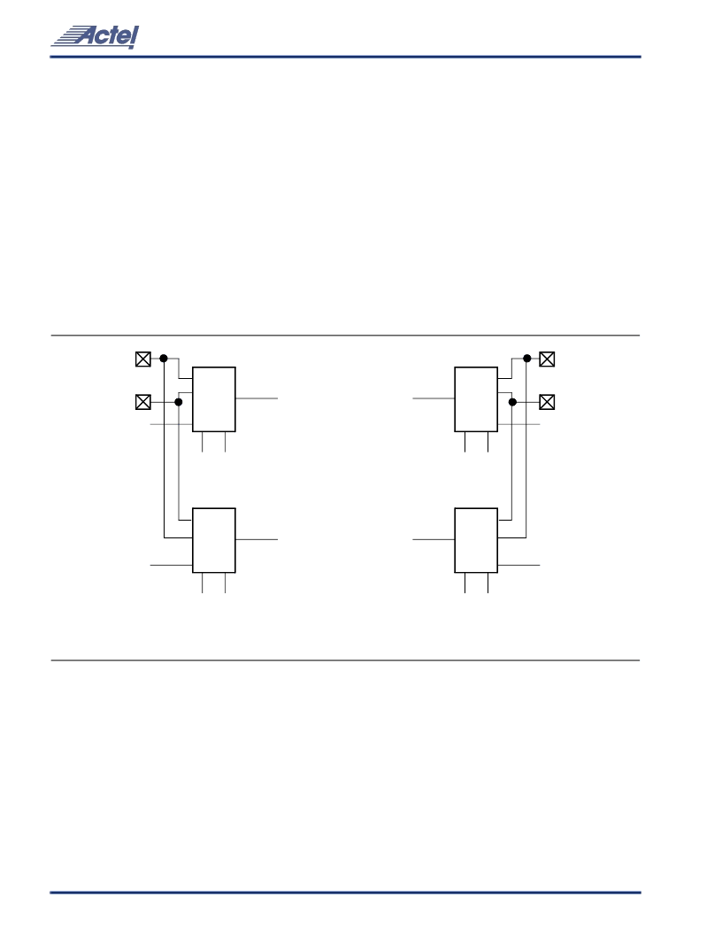
Figure 10
Quadrant Clock Network
Quad
Clock
Module
QCLKA
QCLKB
*QCLK1IN
S0 S1
QCLK1
Quad
Clock
Module
*QCLK2IN
S0 S1
QCLK2
Quad
Clock
Module
QCLKC
QCLKD
*QCLK3IN
S0
S1
QCLK3
Quad
Clock
Module
*QCLK4IN
S0
S1
QCLK4
*QCLK1IN, QCLK2IN, QCLK3IN, and QCLK4IN are internally-generated signals.
相關(guān)PDF資料 |
PDF描述 |
|---|---|
| A40MX04-3PQ100I | Field Programmable Gate Array (FPGA) |
| A40MX04-3PQ100M | Field Programmable Gate Array (FPGA) |
| A40MX04-3VQ80 | Field Programmable Gate Array (FPGA) |
| A40MX04-3VQ80I | Field Programmable Gate Array (FPGA) |
| A40MX04-3VQ80M | Field Programmable Gate Array (FPGA) |
相關(guān)代理商/技術(shù)參數(shù) |
參數(shù)描述 |
|---|---|
| A40MX04-3PQ100I | 功能描述:IC FPGA MX SGL CHIP 6K 100-PQFP RoHS:否 類別:集成電路 (IC) >> 嵌入式 - FPGA(現(xiàn)場(chǎng)可編程門陣列) 系列:MX 標(biāo)準(zhǔn)包裝:90 系列:ProASIC3 LAB/CLB數(shù):- 邏輯元件/單元數(shù):- RAM 位總計(jì):36864 輸入/輸出數(shù):157 門數(shù):250000 電源電壓:1.425 V ~ 1.575 V 安裝類型:表面貼裝 工作溫度:-40°C ~ 125°C 封裝/外殼:256-LBGA 供應(yīng)商設(shè)備封裝:256-FPBGA(17x17) |
| A40MX04-3PQ100M | 制造商:未知廠家 制造商全稱:未知廠家 功能描述:Field Programmable Gate Array (FPGA) |
| A40MX04-3PQG100 | 功能描述:IC FPGA MX SGL CHIP 6K 100-PQFP RoHS:是 類別:集成電路 (IC) >> 嵌入式 - FPGA(現(xiàn)場(chǎng)可編程門陣列) 系列:MX 標(biāo)準(zhǔn)包裝:90 系列:ProASIC3 LAB/CLB數(shù):- 邏輯元件/單元數(shù):- RAM 位總計(jì):36864 輸入/輸出數(shù):157 門數(shù):250000 電源電壓:1.425 V ~ 1.575 V 安裝類型:表面貼裝 工作溫度:-40°C ~ 125°C 封裝/外殼:256-LBGA 供應(yīng)商設(shè)備封裝:256-FPBGA(17x17) |
| A40MX04-3PQG100I | 功能描述:IC FPGA MX SGL CHIP 6K 100-PQFP RoHS:是 類別:集成電路 (IC) >> 嵌入式 - FPGA(現(xiàn)場(chǎng)可編程門陣列) 系列:MX 標(biāo)準(zhǔn)包裝:90 系列:ProASIC3 LAB/CLB數(shù):- 邏輯元件/單元數(shù):- RAM 位總計(jì):36864 輸入/輸出數(shù):157 門數(shù):250000 電源電壓:1.425 V ~ 1.575 V 安裝類型:表面貼裝 工作溫度:-40°C ~ 125°C 封裝/外殼:256-LBGA 供應(yīng)商設(shè)備封裝:256-FPBGA(17x17) |
| A40MX04-3VQ80 | 功能描述:IC FPGA MX SGL CHIP 6K 80-VQFP RoHS:否 類別:集成電路 (IC) >> 嵌入式 - FPGA(現(xiàn)場(chǎng)可編程門陣列) 系列:MX 標(biāo)準(zhǔn)包裝:90 系列:ProASIC3 LAB/CLB數(shù):- 邏輯元件/單元數(shù):- RAM 位總計(jì):36864 輸入/輸出數(shù):157 門數(shù):250000 電源電壓:1.425 V ~ 1.575 V 安裝類型:表面貼裝 工作溫度:-40°C ~ 125°C 封裝/外殼:256-LBGA 供應(yīng)商設(shè)備封裝:256-FPBGA(17x17) |
發(fā)布緊急采購(gòu),3分鐘左右您將得到回復(fù)。