- 您現(xiàn)在的位置:買賣IC網(wǎng) > PDF目錄362018 > A40MX04-2VQ80I Field Programmable Gate Array (FPGA) PDF資料下載
參數(shù)資料
| 型號: | A40MX04-2VQ80I |
| 英文描述: | Field Programmable Gate Array (FPGA) |
| 中文描述: | 現(xiàn)場可編程門陣列(FPGA) |
| 文件頁數(shù): | 11/116頁 |
| 文件大小: | 3110K |
| 代理商: | A40MX04-2VQ80I |
第1頁第2頁第3頁第4頁第5頁第6頁第7頁第8頁第9頁第10頁當前第11頁第12頁第13頁第14頁第15頁第16頁第17頁第18頁第19頁第20頁第21頁第22頁第23頁第24頁第25頁第26頁第27頁第28頁第29頁第30頁第31頁第32頁第33頁第34頁第35頁第36頁第37頁第38頁第39頁第40頁第41頁第42頁第43頁第44頁第45頁第46頁第47頁第48頁第49頁第50頁第51頁第52頁第53頁第54頁第55頁第56頁第57頁第58頁第59頁第60頁第61頁第62頁第63頁第64頁第65頁第66頁第67頁第68頁第69頁第70頁第71頁第72頁第73頁第74頁第75頁第76頁第77頁第78頁第79頁第80頁第81頁第82頁第83頁第84頁第85頁第86頁第87頁第88頁第89頁第90頁第91頁第92頁第93頁第94頁第95頁第96頁第97頁第98頁第99頁第100頁第101頁第102頁第103頁第104頁第105頁第106頁第107頁第108頁第109頁第110頁第111頁第112頁第113頁第114頁第115頁第116頁
v5.0
11
40MX and 42MX FPGA Families
When a device is operating in BST mode, four I/O pins are
used for the TDI, TDO, TMS, and TCK signals. An active
reset (nTRST) pin is not supported; however, the 42MX
device contain power-on circuitry that resets the boundary
scan circuitry upon power-up.
Table 1
summarizes the
functions of the IEEE 1149.1 BST signals.
JTAG
All SX-A devices are IEEE 1149.1 (JTAG) compliant. SX-A
devices offer superior diagnostic and testing capabilities by
providing JTAG and probing capabilites. These functions
are controlled through the special JTAG pins in conjunction
with the program fuse.
JTAG fuse programmed:
TCK must be terminated
—
logical high or low doesn
’
t
matter (to avoid floating input)
TDI, TMS may float or at logical high (internal pull-up is
present)
TDO may float or connect to TDI of another device (it
’
s an
output)
JTAG fuse not programmed:
TCK, TDI, TDO, TMS are user I/O. If not used, they will be
configured as tristated output.
BST Instructions
Boundary scan testing within the 42MX devices is controlled
by a Test Access Port (TAP) state machine. The TAP
controller drives the three-bit instruction register, a bypass
register, and the boundary scan data registers within the
device. The TAP controller uses the TMS signal to control
the testing of the device. The BST mode is determined by
the bitstream entered on the TMS pin.
Table 2
describes the
test instructions supported by the 42MX devices.
Reset
The TMS pin is equipped with an internal pull-up resistor.
This allows the TAP controller to remain in or return to the
Test-Logic-Reset state when there is no input or when a
logical 1 is on the TMS pin. To reset the controller, TMS
must be HIGH for at least five TCK cycles.
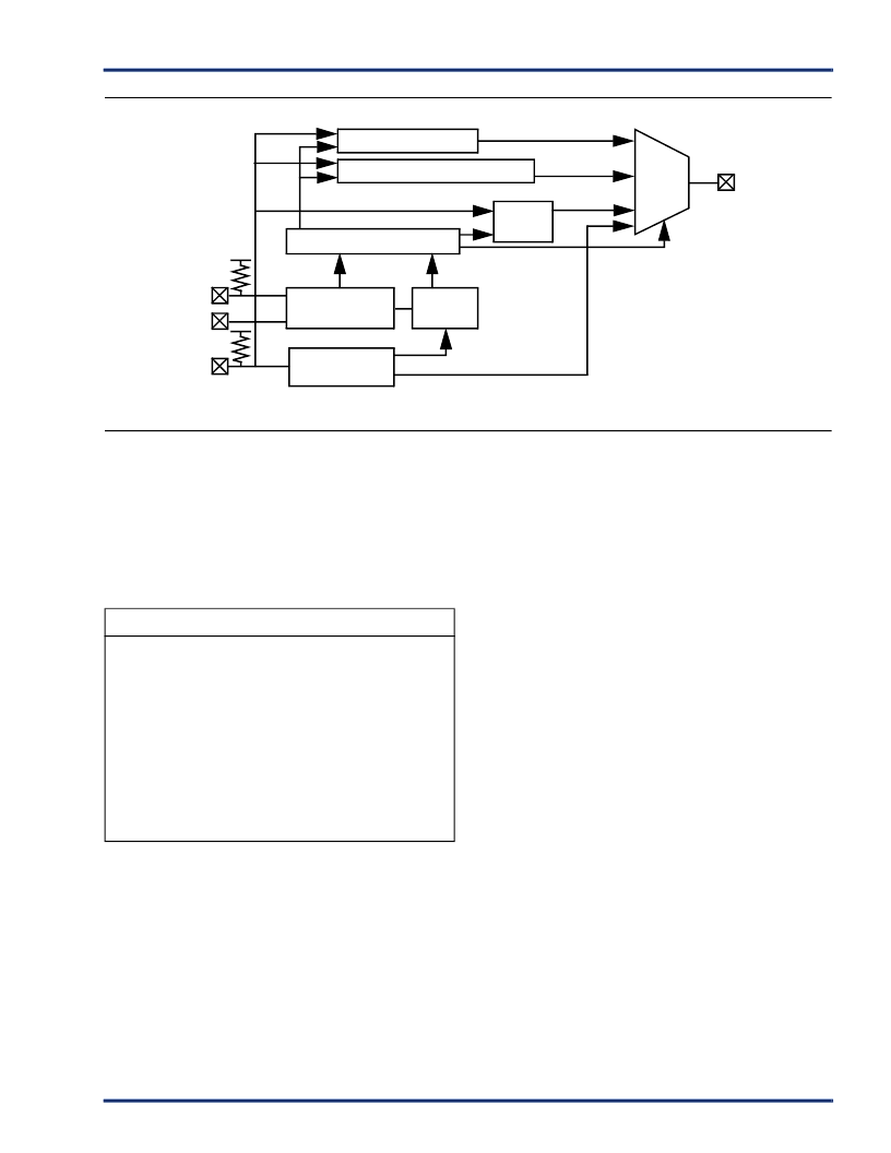
Figure 11
42MX IEEE 1149.1 Boundary Scan Circuitry
JPROBE Register
Boundary Scan Register
Instruction
Decode
Control Logic
TAP Controller
Instruction
Register
Bypass
Register
TMS
TCK
TDI
Output
MUX
TDO
JTAG
JTAG
Table 1
IEEE 1149.1 BST Signals
Signal
Name
Function
TDI
Test Data In
Serial data input for BST
instructions and data. Data is
shifted in on the rising edge of
TCK.
TDO
Test Data
Out
Serial data output for BST
instructions and test data.
TMS
Test Mode
Select
Serial data input for BST mode.
Data is shifted in on the rising
edge of TCK.
TCK
Test Clock
Clock signal to shift the BST
data into the device.
相關PDF資料 |
PDF描述 |
|---|---|
| A40MX04-FPL44M | Field Programmable Gate Array (FPGA) |
| A40MX04-FPL68 | Field Programmable Gate Array (FPGA) |
| A40MX04-FPL68I | Field Programmable Gate Array (FPGA) |
| A40MX04-FPL68M | Field Programmable Gate Array (FPGA) |
| A40MX04-FPL84 | Field Programmable Gate Array (FPGA) |
相關代理商/技術參數(shù) |
參數(shù)描述 |
|---|---|
| A40MX04-2VQ80M | 制造商:未知廠家 制造商全稱:未知廠家 功能描述:Field Programmable Gate Array (FPGA) |
| A40MX04-2VQG80 | 功能描述:IC FPGA MX SGL CHIP 6K 80-VQFP RoHS:是 類別:集成電路 (IC) >> 嵌入式 - FPGA(現(xiàn)場可編程門陣列) 系列:MX 標準包裝:90 系列:ProASIC3 LAB/CLB數(shù):- 邏輯元件/單元數(shù):- RAM 位總計:36864 輸入/輸出數(shù):157 門數(shù):250000 電源電壓:1.425 V ~ 1.575 V 安裝類型:表面貼裝 工作溫度:-40°C ~ 125°C 封裝/外殼:256-LBGA 供應商設備封裝:256-FPBGA(17x17) |
| A40MX04-2VQG80I | 功能描述:IC FPGA MX SGL CHIP 6K 80-VQFP RoHS:是 類別:集成電路 (IC) >> 嵌入式 - FPGA(現(xiàn)場可編程門陣列) 系列:MX 標準包裝:90 系列:ProASIC3 LAB/CLB數(shù):- 邏輯元件/單元數(shù):- RAM 位總計:36864 輸入/輸出數(shù):157 門數(shù):250000 電源電壓:1.425 V ~ 1.575 V 安裝類型:表面貼裝 工作溫度:-40°C ~ 125°C 封裝/外殼:256-LBGA 供應商設備封裝:256-FPBGA(17x17) |
| A40MX04-3PL44 | 功能描述:IC FPGA MX SGL CHIP 6K 44-PLCC RoHS:否 類別:集成電路 (IC) >> 嵌入式 - FPGA(現(xiàn)場可編程門陣列) 系列:MX 標準包裝:90 系列:ProASIC3 LAB/CLB數(shù):- 邏輯元件/單元數(shù):- RAM 位總計:36864 輸入/輸出數(shù):157 門數(shù):250000 電源電壓:1.425 V ~ 1.575 V 安裝類型:表面貼裝 工作溫度:-40°C ~ 125°C 封裝/外殼:256-LBGA 供應商設備封裝:256-FPBGA(17x17) |
| A40MX04-3PL44I | 功能描述:IC FPGA MX SGL CHIP 6K 44-PLCC RoHS:否 類別:集成電路 (IC) >> 嵌入式 - FPGA(現(xiàn)場可編程門陣列) 系列:MX 標準包裝:90 系列:ProASIC3 LAB/CLB數(shù):- 邏輯元件/單元數(shù):- RAM 位總計:36864 輸入/輸出數(shù):157 門數(shù):250000 電源電壓:1.425 V ~ 1.575 V 安裝類型:表面貼裝 工作溫度:-40°C ~ 125°C 封裝/外殼:256-LBGA 供應商設備封裝:256-FPBGA(17x17) |
發(fā)布緊急采購,3分鐘左右您將得到回復。