- 您現(xiàn)在的位置:買賣IC網(wǎng) > PDF目錄379518 > A40MX02 (Electronic Theatre Controls, Inc.) 40MX and 42MX FPGA Families PDF資料下載
參數(shù)資料
| 型號: | A40MX02 |
| 廠商: | Electronic Theatre Controls, Inc. |
| 英文描述: | 40MX and 42MX FPGA Families |
| 中文描述: | 40MX和42MX FPGA系列 |
| 文件頁數(shù): | 80/123頁 |
| 文件大小: | 854K |
| 代理商: | A40MX02 |
第1頁第2頁第3頁第4頁第5頁第6頁第7頁第8頁第9頁第10頁第11頁第12頁第13頁第14頁第15頁第16頁第17頁第18頁第19頁第20頁第21頁第22頁第23頁第24頁第25頁第26頁第27頁第28頁第29頁第30頁第31頁第32頁第33頁第34頁第35頁第36頁第37頁第38頁第39頁第40頁第41頁第42頁第43頁第44頁第45頁第46頁第47頁第48頁第49頁第50頁第51頁第52頁第53頁第54頁第55頁第56頁第57頁第58頁第59頁第60頁第61頁第62頁第63頁第64頁第65頁第66頁第67頁第68頁第69頁第70頁第71頁第72頁第73頁第74頁第75頁第76頁第77頁第78頁第79頁當前第80頁第81頁第82頁第83頁第84頁第85頁第86頁第87頁第88頁第89頁第90頁第91頁第92頁第93頁第94頁第95頁第96頁第97頁第98頁第99頁第100頁第101頁第102頁第103頁第104頁第105頁第106頁第107頁第108頁第109頁第110頁第111頁第112頁第113頁第114頁第115頁第116頁第117頁第118頁第119頁第120頁第121頁第122頁第123頁
40MX and 42MX FPGA Families
1-74
v6.0
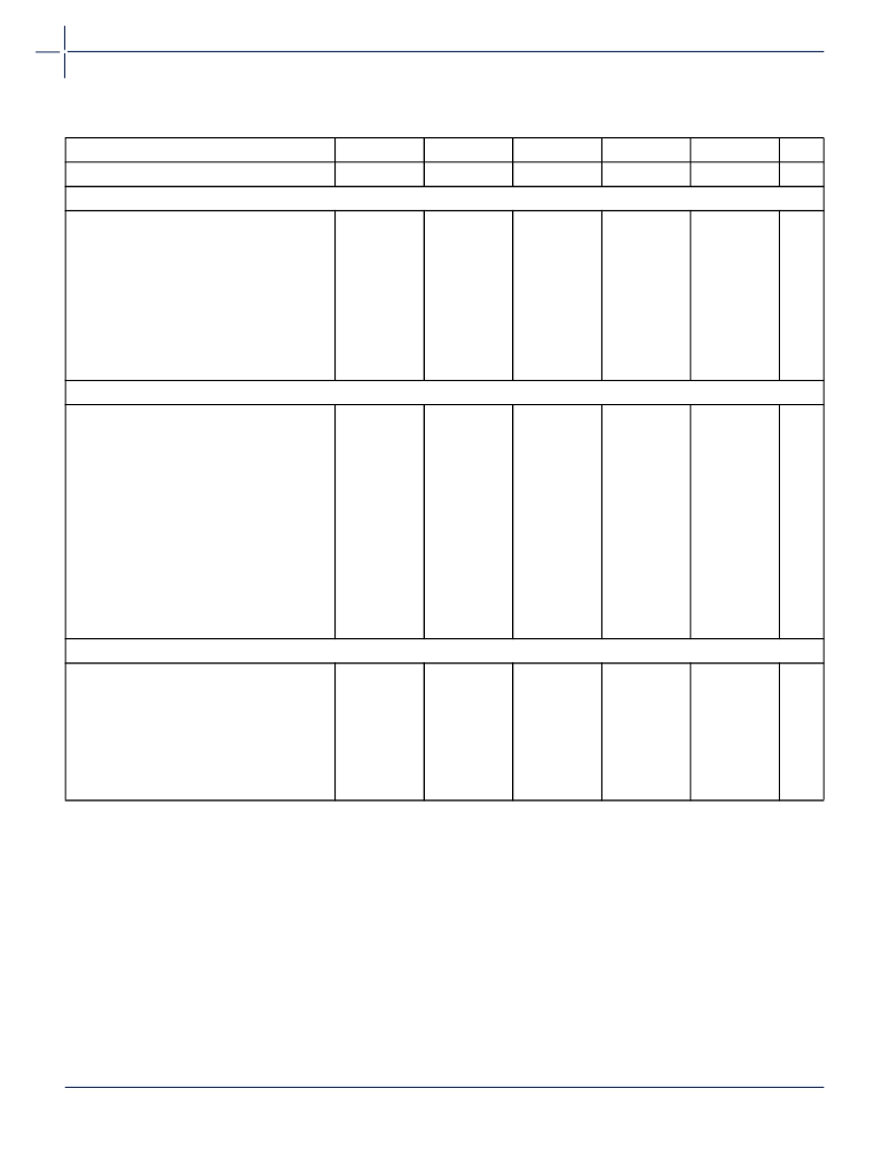
Synchronous SRAM Operations (Continued)
t
ADH
t
RENSU
t
RENH
t
WENSU
t
WENH
t
BENS
t
BENH
Asynchronous SRAM Operations
Address/Data Hold Time
0.0
0.0
0.0
0.0
0.0
ns
Read Enable Set-Up
0.9
1.0
1.1
1.3
1.8
ns
Read Enable Hold
4.8
5.3
6.0
7.0
9.8
ns
Write Enable Set-Up
3.8
4.2
4.8
5.6
7.8
ns
Write Enable Hold
0.0
0.0
0.0
0.0
0.0
ns
Block Enable Set-Up
3.9
4.3
4.9
5.7
8.0
ns
Block Enable Hold
0.0
0.0
0.0
0.0
0.0
ns
t
RPD
t
RDADV
t
ADSU
t
ADH
t
RENSUA
Asynchronous Access Time
11.3
12.6
14.3
16.8
23.5
ns
Read Address Valid
12.3
13.7
15.5
18.2
25.5
ns
Address/Data Set-Up Time
2.3
2.5
2.8
3.4
4.8
ns
Address/Data Hold Time
0.0
0.0
0.0
0.0
0.0
ns
Read Enable Set-Up to Address
Valid
0.9
1.0
1.1
1.3
1.8
ns
t
RENHA
t
WENSU
t
WENH
t
DOH
Input Module Propagation Delays
Read Enable Hold
4.8
5.3
6.0
7.0
9.8
ns
Write Enable Set-Up
3.8
4.2
4.8
5.6
7.8
ns
Write Enable Hold
0.0
0.0
0.0
0.0
0.0
ns
Data Out Hold Time
1.8
2.0
2.1
2.5
3.5
ns
t
INPY
t
INGO
Input Data Pad-to-Y
1.4
1.6
1.8
2.1
3.0
ns
Input Latch Gate-to-
Output
2.0
2.2
2.5
2.9
4.1
ns
t
INH
t
INSU
t
ILA
Notes:
1. For dual-module macros, use t
PD1
+ t
RD1
+ t
PDn
, t
CO
+ t
RD1
+ t
PDn
, or t
PD1
+ t
RD1
+ t
SUD
, whichever is appropriate.
2. Routing delays are for typical designs across worst-case operating conditions. These parameters should be used for estimating
device performance. Post-route timing analysis or simulation is required to determine actual performance.
3. Data applies to macros based on the S-module. Timing parameters for sequential macros constructed from C-modules can be
obtained from the Timer utility.
4. Set-up and hold timing parameters for the Input Buffer Latch are defined with respect to the PAD and the D input. External setup/
hold timing parameters must account for delay from an external PAD signal to the G inputs. Delay from an external PAD signal to
the G input subtracts (adds) to the internal setup (hold) time.
5. Delays based on 35 pF loading.
Input Latch Hold
0.0
0.0
0.0
0.0
0.0
ns
Input Latch Set-Up
0.7
0.7
0.8
1.0
1.4
ns
Latch Active Pulse Width
6.5
7.3
8.2
9.7
13.5
ns
Table 39
A42MX36 Timing Characteristics (Nominal 3.3V Operation) (Continued)
(Worst-Case Commercial Conditions, V
CCA
= 3.0V, T
J
= 70°C)
‘–3’ Speed
‘–2’ Speed
‘–1’ Speed
‘Std’ Speed
‘–F’ Speed
Parameter Description
Min.
Max.
Min.
Max.
Min.
Max.
Min.
Max.
Min.
Max. Units
相關(guān)PDF資料 |
PDF描述 |
|---|---|
| A40MX04 | 40MX and 42MX FPGA Families |
| A42MX02-1PL100ES | 40MX and 42MX FPGA Families |
| A42MX02-1PL100I | 40MX and 42MX FPGA Families |
| A42MX02-1PL100M | 40MX and 42MX FPGA Families |
| A42MX02-1PQ100I | 40MX and 42MX FPGA Families |
相關(guān)代理商/技術(shù)參數(shù) |
參數(shù)描述 |
|---|---|
| A40MX02-1BG100 | 制造商:ACTEL 制造商全稱:Actel Corporation 功能描述:40MX and 42MX FPGA Families |
| A40MX02-1BG100ES | 制造商:ACTEL 制造商全稱:Actel Corporation 功能描述:40MX and 42MX FPGA Families |
| A40MX02-1BG100I | 制造商:ACTEL 制造商全稱:Actel Corporation 功能描述:40MX and 42MX FPGA Families |
| A40MX02-1BG100M | 制造商:ACTEL 制造商全稱:Actel Corporation 功能描述:40MX and 42MX FPGA Families |
| A40MX02-1CQ100 | 制造商:ACTEL 制造商全稱:Actel Corporation 功能描述:40MX and 42MX FPGA Families |
發(fā)布緊急采購,3分鐘左右您將得到回復(fù)。