- 您現(xiàn)在的位置:買賣IC網(wǎng) > PDF目錄362018 > A40MX02-3VQ80M Field Programmable Gate Array (FPGA) PDF資料下載
參數(shù)資料
| 型號: | A40MX02-3VQ80M |
| 英文描述: | Field Programmable Gate Array (FPGA) |
| 中文描述: | 現(xiàn)場可編程門陣列(FPGA) |
| 文件頁數(shù): | 14/116頁 |
| 文件大小: | 3110K |
| 代理商: | A40MX02-3VQ80M |
第1頁第2頁第3頁第4頁第5頁第6頁第7頁第8頁第9頁第10頁第11頁第12頁第13頁當前第14頁第15頁第16頁第17頁第18頁第19頁第20頁第21頁第22頁第23頁第24頁第25頁第26頁第27頁第28頁第29頁第30頁第31頁第32頁第33頁第34頁第35頁第36頁第37頁第38頁第39頁第40頁第41頁第42頁第43頁第44頁第45頁第46頁第47頁第48頁第49頁第50頁第51頁第52頁第53頁第54頁第55頁第56頁第57頁第58頁第59頁第60頁第61頁第62頁第63頁第64頁第65頁第66頁第67頁第68頁第69頁第70頁第71頁第72頁第73頁第74頁第75頁第76頁第77頁第78頁第79頁第80頁第81頁第82頁第83頁第84頁第85頁第86頁第87頁第88頁第89頁第90頁第91頁第92頁第93頁第94頁第95頁第96頁第97頁第98頁第99頁第100頁第101頁第102頁第103頁第104頁第105頁第106頁第107頁第108頁第109頁第110頁第111頁第112頁第113頁第114頁第115頁第116頁
40MX and 42MX FPGA Families
14
v5.0
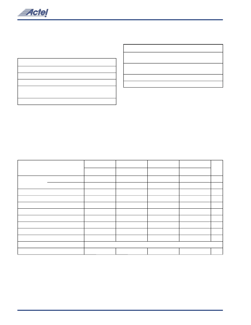
3.3V Operating Conditions
Absolute Maximum Ratings
1
V
CC
= V
CCA
and V
CCI
Free Air Temperature Range
Recommended Operating Conditions
Symbol
Parameter
Limits
Units
V
CC
V
I
V
O
DC Supply Voltage
–
0.5 to +7.0
V
Input Voltage
–
0.5 to V
CC
+0.5
–
0.5 to V
CC
+0.5
V
Output Voltage
V
I
IO
I/O Source Sink
Current
2
±20
mA
T
STG
Notes:
1.
Storage Temperature
–
65 to +150
°
C
Stresses beyond those listed under
“
Absolute Maximum
Ratings
”
may cause permanent damage to the device.
Exposure to absolute maximum rated conditions for extended
periods may affect device reliability. Devices should not be
operated outside the Recommended Operating Conditions.
Device inputs are normally high impedance and draw
extremely low current. However, when input voltage is greater
than V
CC
+ 0.5V or less than GND
–
0.5V, the internal protection
diodes will forward-bias and can draw excessive current.
2.
Parameter
Commercial Industrial
Military
Units
Temperature
Range
1
0 to
+70
–
40 to
+85
–
55 to
+125
°
C
Power Supply
Tolerance
±5
±10
±10
%V
V
CCI
V
CCA
Note:
1.
3.0 to 3.6
3.0 to 3.6
3.0 to 3.6
V
3.0 to 3.6
3.0 to 3.6
3.0 to 3.6
V
Ambient temperature (T
A
) is used for commercial, and
industrial; case temperature (T
C
) is used for military.
Electrical Specifications
Parameter
Commercial
Commercial
‘–
F
’
Industrial
Military
Units
Min.
Max.
Min.
Max.
Min.
Max.
Min.
Max.
V
OH1
(I
OH
=
–
4 mA)
(I
OH
=
–
3.2 mA)
(I
OL
= 6 mA)
2.15
2.15
2.4
2.4
V
2.4
2.4
V
V
OL1
V
IL
V
IH
I
IL
I
IH
Input Transition Time t
R
, t
F2
C
IO
I/O Capacitance
2, 3
Standby Current, I
CC4
I
CC(D)
Dynamic V
CC
Supply Current
Low Power Mode Standby Current
0.4
0.4
0.48
0.48
V
–
0.3
0.8
–
0.3
0.8
–
0.3
0.8
–
0.3
0.8
V
2.0
V
CC
+ 0.3
–
10
2.0
V
CC
+ 0.3
–
10
2.0
V
CC
+ 0.3
–
10
2.0
V
CC
+ 0.3
–
10
V
μA
–
10
–
10
–
10
–
10
μA
500
500
500
500
ns
10
10
10
10
pF
Notes 5 & 6
25
Notes 6 & 7
25
mA
See the
“
Power Dissipation
”
section on
page 18
.
Note 8
I
CC
–
5.0
I
CC
–
5.0
I
CC
–
5.0
mA
Notes:
1.
2.
3.
4.
5.
6.
7.
8.
Only one output IV curve tested at a time. V
CC
= min.
Not tested, for information only.
Includes worst-case 84-pin PLCC package capacitance. V
OUT
= 0 V, f = 1 MHz.
All outputs unloaded. All inputs = V
CC
or GND.
A40MX02 and A40MX04 I
CC
= 3 mA, A42MX09 I
CC
= 5 mA, A42MX16 I
CC
= 6 mA, A42MX24 and A42MX36 I
CC
= 25 mA.
I
CC
Max = 1.5mA is available by special request. Contact your Actel Sales representative for additional information.
A40MX02 and A40MX04 I
CC
= 10 mA, A42MX09, A42MX16, A42MX24, and A42MX36 I
CC
= 25 mA.
In Low Power Mode, A42MX09 I
CC
= 15 μA; A42MX16, A42MX24, A42MX36 I
CC
= 50 μA. A40MX02 and A40MX04 = N/A.
相關PDF資料 |
PDF描述 |
|---|---|
| A40MX02-FPL44 | Field Programmable Gate Array (FPGA) |
| A40MX02-FPL44I | Field Programmable Gate Array (FPGA) |
| A40MX04-1VQ80M | Field Programmable Gate Array (FPGA) |
| A40MX04-2PL44 | Field Programmable Gate Array (FPGA) |
| A40MX04-2PL44I | Field Programmable Gate Array (FPGA) |
相關代理商/技術參數(shù) |
參數(shù)描述 |
|---|---|
| A40MX02-3VQG80 | 功能描述:IC FPGA MX SGL CHIP 3K 80-VQFP RoHS:是 類別:集成電路 (IC) >> 嵌入式 - FPGA(現(xiàn)場可編程門陣列) 系列:MX 標準包裝:90 系列:ProASIC3 LAB/CLB數(shù):- 邏輯元件/單元數(shù):- RAM 位總計:36864 輸入/輸出數(shù):157 門數(shù):250000 電源電壓:1.425 V ~ 1.575 V 安裝類型:表面貼裝 工作溫度:-40°C ~ 125°C 封裝/外殼:256-LBGA 供應商設備封裝:256-FPBGA(17x17) |
| A40MX02-3VQG80I | 功能描述:IC FPGA MX SGL CHIP 3K 80-VQFP RoHS:是 類別:集成電路 (IC) >> 嵌入式 - FPGA(現(xiàn)場可編程門陣列) 系列:MX 標準包裝:90 系列:ProASIC3 LAB/CLB數(shù):- 邏輯元件/單元數(shù):- RAM 位總計:36864 輸入/輸出數(shù):157 門數(shù):250000 電源電壓:1.425 V ~ 1.575 V 安裝類型:表面貼裝 工作溫度:-40°C ~ 125°C 封裝/外殼:256-LBGA 供應商設備封裝:256-FPBGA(17x17) |
| A40MX02-BG100 | 制造商:ACTEL 制造商全稱:Actel Corporation 功能描述:40MX and 42MX FPGA Families |
| A40MX02-BG100ES | 制造商:ACTEL 制造商全稱:Actel Corporation 功能描述:40MX and 42MX FPGA Families |
| A40MX02-BG100I | 制造商:ACTEL 制造商全稱:Actel Corporation 功能描述:40MX and 42MX FPGA Families |
發(fā)布緊急采購,3分鐘左右您將得到回復。