- 您現(xiàn)在的位置:買賣IC網(wǎng) > PDF目錄294787 > A32400DX-2BG313I FPGA, 2526 CLBS, 40000 GATES, PBGA313 PDF資料下載
參數(shù)資料
| 型號(hào): | A32400DX-2BG313I |
| 元件分類: | FPGA |
| 英文描述: | FPGA, 2526 CLBS, 40000 GATES, PBGA313 |
| 封裝: | BGA-313 |
| 文件頁(yè)數(shù): | 18/22頁(yè) |
| 文件大小: | 217K |
| 代理商: | A32400DX-2BG313I |
第1頁(yè)第2頁(yè)第3頁(yè)第4頁(yè)第5頁(yè)第6頁(yè)第7頁(yè)第8頁(yè)第9頁(yè)第10頁(yè)第11頁(yè)第12頁(yè)第13頁(yè)第14頁(yè)第15頁(yè)第16頁(yè)第17頁(yè)當(dāng)前第18頁(yè)第19頁(yè)第20頁(yè)第21頁(yè)第22頁(yè)

5
3200DX Field Programmable Gate Arrays – The System Logic Integrator Family
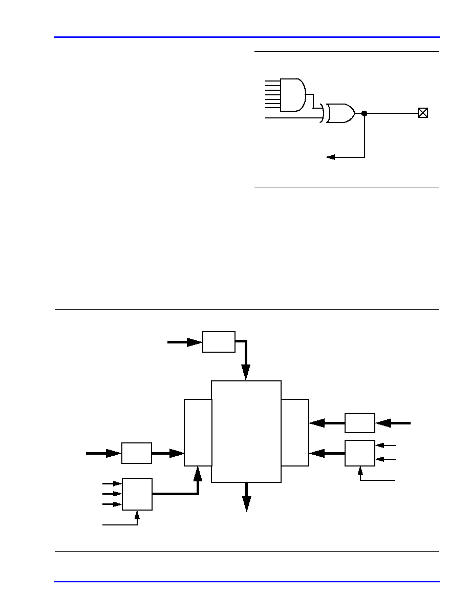
analogous to the wide-input AND term in a CPLD or PAL
device. The output of the D-module has a programmable
inverter for active HIGH or LOW assertion. The D-module
output is hardwired to an output pin or can be fed back into
the array to be incorporated into other logic.
Dual-Port SRAM Modules
The 3200DX dual-port SRAM modules have been optimized
for synchronous or asynchronous applications. The SRAM
modules are arranged in 256 bit blocks which can be
configured as 32 x 8 or 64 x 4 (refer to Table 1 for the number
of SRAM modules within a particular device). The SRAM
module block structure allows them to be cascaded together
to form user-definable memory spaces. Resources within the
3200DX architecture allow the SRAM modules to be
cascaded together without incurring an additional delay
penalty. A block diagram of the 3200DX dual-port SRAM
block is shown in Figure 4.
The 3200DX SRAM blocks are true dual-port structures
containing independent READ and WRITE logic. The
SRAM blocks contain six bits of read and write addressing
(RDAD[5:0] and WRAD[5:0] respectively) for 64x4 bit
blocks. When configured in byte mode, the highest order
address bits (RDAD5 and WRAD5) are not used. The read
and write ports of the SRAM blocks contain independent
clocks (RCLK and WCLK) with programmable polarities
offering active HIGH or LOW implementation. The write
and read ports of the SRAM block have eight data inputs
(WD[7:0]) and eight outputs (RD[7:0]). The SRAM block
outputs are connected to segmented vertical routing tracks.
The 3200DX dual-port SRAM blocks are ideal for
high-speed buffered applications such as DMA controllers
and FIFO and LIFO queues. Actel’s ACTgen Macro Builder
provides the capability to quickly design memory elements,
such as FIFOs, LIFOs, and RAM arrays which can be
included in any 3200DX design. Additionally, unused SRAM
blocks can be used to implement registers for other logic
within the design.
Figure 3 D-Module Implementation
7 inputs
hardwire to I/O
feedback to array
Programmable
inverter
Figure 4 Dual-Port SRAM Module
SRAM Module
32 x 8 or 64 x 4
(256 bits)
Read
Port
Logic
Write
Port
Logic
RD[7:0]
Routing Tracks
Latches
Read
Logic
[5:0]
RDAD[5:0]
LEN
REN
RCLK
Latches
WD[7:0]
Latches
WRAD[5:0]
Write
Logic
MODE
BLKEN
WEN
WCLK
[5:0]
[7:0]
相關(guān)PDF資料 |
PDF描述 |
|---|---|
| A32400DX-2PQ240C | FPGA, 2526 CLBS, 40000 GATES, PQFP240 |
| A32400DX-2PQ240I | FPGA, 2526 CLBS, 40000 GATES, PQFP240 |
| A32400DX-BG313C | FPGA, 2526 CLBS, 40000 GATES, PBGA313 |
| A32400DX-BG313I | FPGA, 2526 CLBS, 40000 GATES, PBGA313 |
| A32400DX-PQ240C | FPGA, 2526 CLBS, 40000 GATES, PQFP240 |
相關(guān)代理商/技術(shù)參數(shù) |
參數(shù)描述 |
|---|---|
| A32400DX-2RQ240C | 制造商:未知廠家 制造商全稱:未知廠家 功能描述:Field Programmable Gate Array (FPGA) |
| A32400DX-2RQ240I | 制造商:未知廠家 制造商全稱:未知廠家 功能描述:Field Programmable Gate Array (FPGA) |
| A32400DX-3RQ240C | 制造商:未知廠家 制造商全稱:未知廠家 功能描述:Field Programmable Gate Array (FPGA) |
| A32400DX-3RQ240I | 制造商:未知廠家 制造商全稱:未知廠家 功能描述:Field Programmable Gate Array (FPGA) |
| A32400DX-FRQ240C | 制造商:未知廠家 制造商全稱:未知廠家 功能描述:Field Programmable Gate Array (FPGA) |
發(fā)布緊急采購(gòu),3分鐘左右您將得到回復(fù)。