- 您現(xiàn)在的位置:買賣IC網(wǎng) > PDF目錄294787 > A3185LU SPECIALTY ANALOG CIRCUIT, PSIP3 PDF資料下載
參數(shù)資料
| 型號: | A3185LU |
| 元件分類: | 模擬信號調(diào)理 |
| 英文描述: | SPECIALTY ANALOG CIRCUIT, PSIP3 |
| 封裝: | MINI, PLASTIC, SIP-3 |
| 文件頁數(shù): | 4/8頁 |
| 文件大?。?/td> | 173K |
| 代理商: | A3185LU |

3185 THRU 3189
HALL-EFFECT LATCHES
FOR HIGH-TEMPERATURE
OPERATION
115 Northeast Cutoff, Box 15036
Worcester, Massachusetts 01615-0036 (508) 853-5000
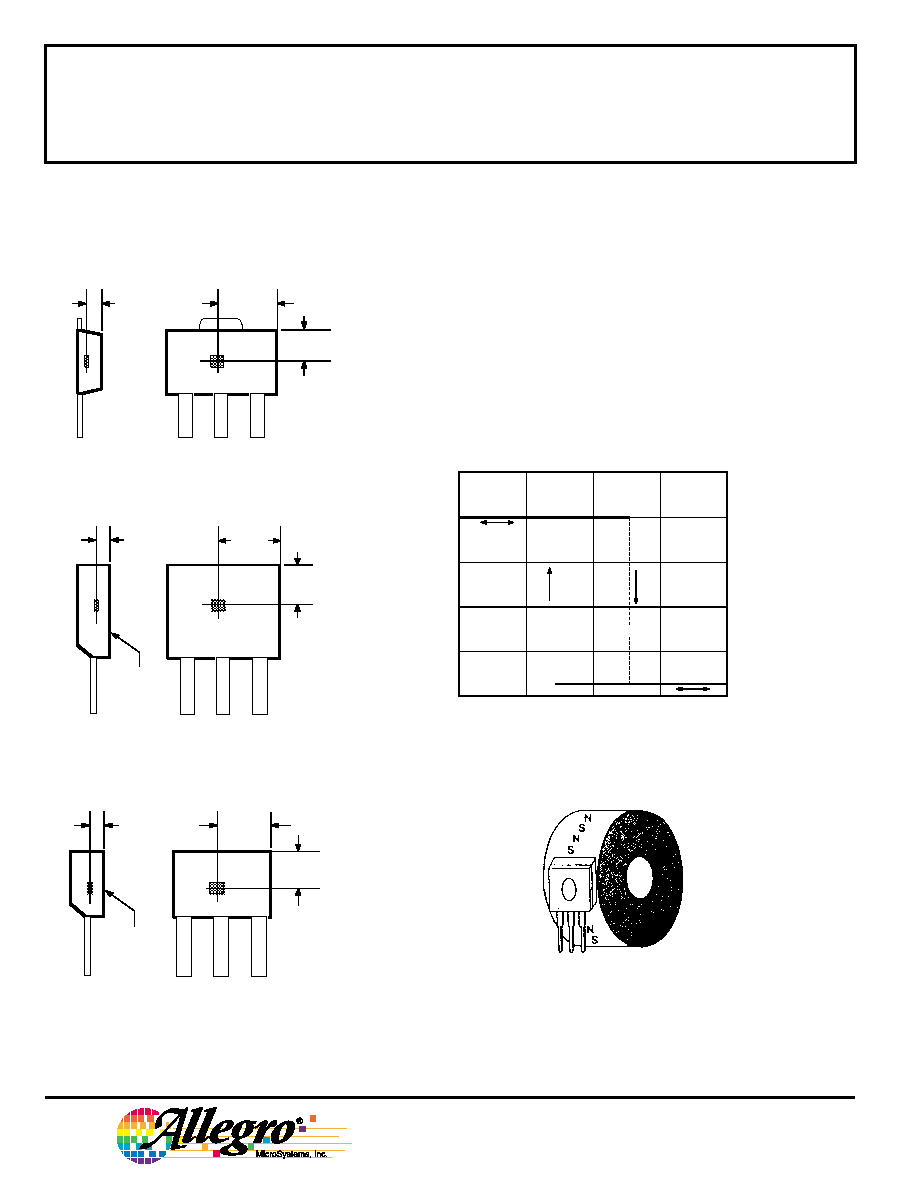
SENSOR LOCATIONS
(
±0.005” [0.13 mm] die placement)
Allegro
Package Designators “LT”
1
3
2
Dwg. MH-008-4C
0.0305"
0.775 mm
NOM
ACTIVE AREA DEPTH
0.050"
1.27 mm
0.090"
2.27 mm
A
Package Designator “U”
1
3
2
Dwg. MH-002-7C
0.0165"
0.42 mm
NOM
BRANDED
SURFACE
ACTIVE AREA DEPTH
0.077"
1.96 mm
0.092"
2.33 mm
A
Package Designators “UA” and "UA-TL"
1
3
2
Dwg. MH-011-4C
0.0195"
0.50 mm
NOM
BRANDED
SURFACE
ACTIVE AREA DEPTH
0.083"
2.10 mm
0.060"
1.51 mm
A
The simplest form of magnet that will operate these devices is a ring
magnet, as shown below. Other methods of operation are possible.
Dwg. A-11,899
OPERATION
In operation, the output transistor is OFF until the strength of the mag-
netic field perpendicular to the surface of the chip exceeds the threshold or
operate point (BOP). When the field strength exceeds BOP, the output transis-
tor switches ON and is capable of sinking 25 mA of current.
The output transistor switches OFF when magnetic field reversal results
in a magnetic flux density below the OFF threshold (BRP). This is illustrated
in the transfer characteristics graph (A3187* shown).
Note that the device latches; that is, a south pole of sufficient strength
will turn the device ON. Removal of the south pole will leave the device ON.
The presence of a north pole of sufficient strength is required to turn the
device OFF. Powering up in the absence of a magnetic field (less than BOP
and higher than BRP) will allow an indeterminate output state. The correct
state is warranted after the first excursion beyond BOP or BRP.
APPLICATIONS INFORMATION
Extensive applications information on magnets and Hall-effect sensors is
also available in the Allegro Integrated and Discrete Semiconductors Data
Book or Application Note 27701.
30 V
MAX
0+B
0
OUTPUT
VOLTAGE
IN
VOLTS
FLUX DENSITY
Dwg. GH-034-4
-B
RP
B
VOUT(SAT)
BB
V
OP
B
Although sensor location is accurate to three
sigma for a particular design, product improve-
ments may result in small changes to sensor
location.
相關(guān)PDF資料 |
PDF描述 |
|---|---|
| A32200DX-1BGG240C | FPGA, 2502 CLBS, 20000 GATES, PBGA240 |
| A32200DX-1BGG240I | FPGA, 2502 CLBS, 20000 GATES, PBGA240 |
| A32200DX-1BGG432C | FPGA, 2502 CLBS, 20000 GATES, PBGA432 |
| A32200DX-1BGG432I | FPGA, 2502 CLBS, 20000 GATES, PBGA432 |
| A32200DX-2BGG240C | FPGA, 2502 CLBS, 20000 GATES, PBGA240 |
相關(guān)代理商/技術(shù)參數(shù) |
參數(shù)描述 |
|---|---|
| A3185LUA | 制造商:ALLEGRO 制造商全稱:Allegro MicroSystems 功能描述:HALL-EFFECT LATCHES FOR HIGH-TEMPERATURE OPERATION |
| A3185SLL | 制造商:未知廠家 制造商全稱:未知廠家 功能描述:Hall-Effect Switch |
| A3185SLT | 制造商:未知廠家 制造商全稱:未知廠家 功能描述:Hall-Effect Switch |
| A3185SU | 制造商:未知廠家 制造商全稱:未知廠家 功能描述:Hall-Effect Switch |
| A3185SUA | 制造商:未知廠家 制造商全稱:未知廠家 功能描述:Hall-Effect Switch |
發(fā)布緊急采購,3分鐘左右您將得到回復。