- 您現(xiàn)在的位置:買賣IC網(wǎng) > PDF目錄4180 > A14V40A-PL84C (Microsemi SoC)IC FPGA 4K GATES 3.3V 84-PLCC PDF資料下載
參數(shù)資料
| 型號: | A14V40A-PL84C |
| 廠商: | Microsemi SoC |
| 文件頁數(shù): | 89/90頁 |
| 文件大小: | 0K |
| 描述: | IC FPGA 4K GATES 3.3V 84-PLCC |
| 產(chǎn)品變化通告: | A1440A Family Discontinuation 24/Jan/2012 |
| 標(biāo)準(zhǔn)包裝: | 16 |
| 系列: | ACT™ 3 |
| LAB/CLB數(shù): | 564 |
| 輸入/輸出數(shù): | 70 |
| 門數(shù): | 4000 |
| 電源電壓: | 3 V ~ 3.6 V |
| 安裝類型: | 表面貼裝 |
| 工作溫度: | 0°C ~ 70°C |
| 封裝/外殼: | 84-LCC(J 形引線) |
| 供應(yīng)商設(shè)備封裝: | 84-PLCC(29.31x29.31) |
第1頁第2頁第3頁第4頁第5頁第6頁第7頁第8頁第9頁第10頁第11頁第12頁第13頁第14頁第15頁第16頁第17頁第18頁第19頁第20頁第21頁第22頁第23頁第24頁第25頁第26頁第27頁第28頁第29頁第30頁第31頁第32頁第33頁第34頁第35頁第36頁第37頁第38頁第39頁第40頁第41頁第42頁第43頁第44頁第45頁第46頁第47頁第48頁第49頁第50頁第51頁第52頁第53頁第54頁第55頁第56頁第57頁第58頁第59頁第60頁第61頁第62頁第63頁第64頁第65頁第66頁第67頁第68頁第69頁第70頁第71頁第72頁第73頁第74頁第75頁第76頁第77頁第78頁第79頁第80頁第81頁第82頁第83頁第84頁第85頁第86頁第87頁第88頁當(dāng)前第89頁第90頁
R e visio n 3
2 -1
2 – Detailed Specifications
This section of the datasheet is meant to familiarize the user with the architecture of the ACT 3 family of
FPGA devices. A generic description of the family will be presented first, followed by a detailed
description of the logic blocks, the routing structure, the antifuses, and the special function circuits. The
on-chip circuitry required to program the devices is not covered.
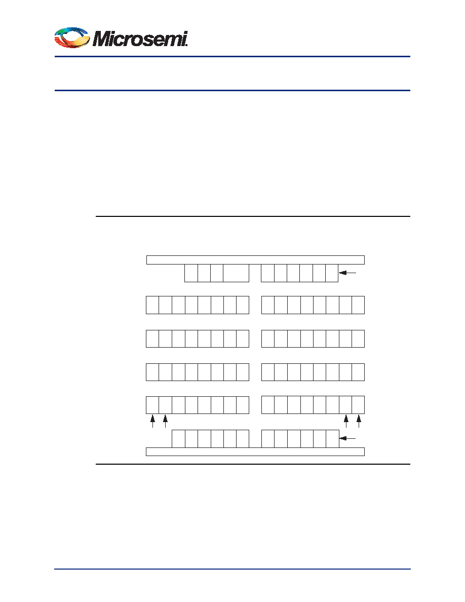
Topology
The ACT 3 family architecture is composed of six key elements: Logic modules, I/O modules, I/O Pad
Drivers, Routing Tracks, Clock Networks, and Programming and Test Circuits. The basic structure is
similar for all devices in the family, differing only in the number of rows, columns, and I/Os. The array
itself consists of alternating rows of modules and channels. The logic modules and channels are in the
center of the array; the I/O modules are located along the array periphery. A simplified floor plan is
depicted in Figure 2-1.
Figure 2-1
Generalized Floor Plan of ACT 3 Device
IO
C
SC
S
IO
C
SC
S
IO
C
SC
S
IO
C
BIO IO
IO
BIN S
C
S
IO
BIN S
C
S
IO
BIN S
C
S
IO
CLKM
IO
BIN S
C
IO
CS
SC
S
IO
C
An Array with
n rows and m columns
Top I/Os
Bottom I/Os
Left I/Os
Right I/Os
Rows
n+1
n
n–1
2
1
0
Channels
n+1
n
n–1
2
1
0
n+2
0
1
2
3
4
5
c–1
c
c+1
m m+1 m+2 m+3
Columns
相關(guān)PDF資料 |
PDF描述 |
|---|---|
| ABB106DHHT-S578 | EDGECARD 212POS .050 SLD W/POSTS |
| A14V40A-PLG84C | IC FPGA 4K GATES 3.3V 84-PLCC |
| A1225A-1PL84I | IC FPGA 2500 GATES 84-PLCC IND |
| A1225A-PL84C | IC FPGA 2500 GATES 84-PLCC COM |
| ESC49DTEI | CONN EDGECARD 98POS .100 EYELET |
相關(guān)代理商/技術(shù)參數(shù) |
參數(shù)描述 |
|---|---|
| A14V40A-PLG84C | 功能描述:IC FPGA 4K GATES 3.3V 84-PLCC RoHS:是 類別:集成電路 (IC) >> 嵌入式 - FPGA(現(xiàn)場可編程門陣列) 系列:ACT™ 3 產(chǎn)品變化通告:XC4000(E,L) Discontinuation 01/April/2002 標(biāo)準(zhǔn)包裝:24 系列:XC4000E/X LAB/CLB數(shù):100 邏輯元件/單元數(shù):238 RAM 位總計(jì):3200 輸入/輸出數(shù):80 門數(shù):3000 電源電壓:4.5 V ~ 5.5 V 安裝類型:表面貼裝 工作溫度:-40°C ~ 100°C 封裝/外殼:120-BCBGA 供應(yīng)商設(shè)備封裝:120-CPGA(34.55x34.55) |
| A14V40A-PQ160C | 功能描述:IC FPGA 4K GATES 3.3V 160-PQFP RoHS:否 類別:集成電路 (IC) >> 嵌入式 - FPGA(現(xiàn)場可編程門陣列) 系列:ACT™ 3 產(chǎn)品變化通告:XC4000(E,L) Discontinuation 01/April/2002 標(biāo)準(zhǔn)包裝:24 系列:XC4000E/X LAB/CLB數(shù):100 邏輯元件/單元數(shù):238 RAM 位總計(jì):3200 輸入/輸出數(shù):80 門數(shù):3000 電源電壓:4.5 V ~ 5.5 V 安裝類型:表面貼裝 工作溫度:-40°C ~ 100°C 封裝/外殼:120-BCBGA 供應(yīng)商設(shè)備封裝:120-CPGA(34.55x34.55) |
| A14V40A-PQG160C | 功能描述:IC FPGA 4K GATES 3.3V 160-PQFP RoHS:是 類別:集成電路 (IC) >> 嵌入式 - FPGA(現(xiàn)場可編程門陣列) 系列:ACT™ 3 產(chǎn)品變化通告:XC4000(E,L) Discontinuation 01/April/2002 標(biāo)準(zhǔn)包裝:24 系列:XC4000E/X LAB/CLB數(shù):100 邏輯元件/單元數(shù):238 RAM 位總計(jì):3200 輸入/輸出數(shù):80 門數(shù):3000 電源電壓:4.5 V ~ 5.5 V 安裝類型:表面貼裝 工作溫度:-40°C ~ 100°C 封裝/外殼:120-BCBGA 供應(yīng)商設(shè)備封裝:120-CPGA(34.55x34.55) |
| A14V40A-TQ176C | 功能描述:IC FPGA 4K GATES 3.3V 176-TQFP RoHS:否 類別:集成電路 (IC) >> 嵌入式 - FPGA(現(xiàn)場可編程門陣列) 系列:ACT™ 3 產(chǎn)品變化通告:XC4000(E,L) Discontinuation 01/April/2002 標(biāo)準(zhǔn)包裝:24 系列:XC4000E/X LAB/CLB數(shù):100 邏輯元件/單元數(shù):238 RAM 位總計(jì):3200 輸入/輸出數(shù):80 門數(shù):3000 電源電壓:4.5 V ~ 5.5 V 安裝類型:表面貼裝 工作溫度:-40°C ~ 100°C 封裝/外殼:120-BCBGA 供應(yīng)商設(shè)備封裝:120-CPGA(34.55x34.55) |
| A14V40A-TQG176C | 功能描述:IC FPGA 4K GATES 3.3V 176-TQFP RoHS:是 類別:集成電路 (IC) >> 嵌入式 - FPGA(現(xiàn)場可編程門陣列) 系列:ACT™ 3 產(chǎn)品變化通告:XC4000(E,L) Discontinuation 01/April/2002 標(biāo)準(zhǔn)包裝:24 系列:XC4000E/X LAB/CLB數(shù):100 邏輯元件/單元數(shù):238 RAM 位總計(jì):3200 輸入/輸出數(shù):80 門數(shù):3000 電源電壓:4.5 V ~ 5.5 V 安裝類型:表面貼裝 工作溫度:-40°C ~ 100°C 封裝/外殼:120-BCBGA 供應(yīng)商設(shè)備封裝:120-CPGA(34.55x34.55) |
發(fā)布緊急采購,3分鐘左右您將得到回復(fù)。