- 您現(xiàn)在的位置:買(mǎi)賣(mài)IC網(wǎng) > PDF目錄122717 > 9ERS3165BGILF (INTEGRATED DEVICE TECHNOLOGY INC) 400 MHz, PROC SPECIFIC CLOCK GENERATOR, PDSO64 PDF資料下載
參數(shù)資料
| 型號(hào): | 9ERS3165BGILF |
| 廠商: | INTEGRATED DEVICE TECHNOLOGY INC |
| 元件分類(lèi): | 時(shí)鐘產(chǎn)生/分配 |
| 英文描述: | 400 MHz, PROC SPECIFIC CLOCK GENERATOR, PDSO64 |
| 封裝: | 6.10 MM, 0.50 MM PITCH, ROHS COMPLIANT, TSSOP-64 |
| 文件頁(yè)數(shù): | 23/26頁(yè) |
| 文件大小: | 319K |
| 代理商: | 9ERS3165BGILF |
第1頁(yè)第2頁(yè)第3頁(yè)第4頁(yè)第5頁(yè)第6頁(yè)第7頁(yè)第8頁(yè)第9頁(yè)第10頁(yè)第11頁(yè)第12頁(yè)第13頁(yè)第14頁(yè)第15頁(yè)第16頁(yè)第17頁(yè)第18頁(yè)第19頁(yè)第20頁(yè)第21頁(yè)第22頁(yè)當(dāng)前第23頁(yè)第24頁(yè)第25頁(yè)第26頁(yè)
IDTTM
Embedded 64-Pin Industrial Temperature Range CK505 Compatible Clock
1613B—01/25/10
ICS9ERS3165
Embedded 64-Pin Industrial Temperature Range CK505 Compatible Clock
6
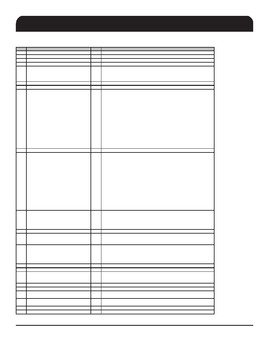
MLF Pin Description
Pin#
Pin Name
TYPE DESCRIPTION
1
GNDREF
PWR Ground pin for crystal oscillator circuit
2
X2
OUT Crystal output, nominally 14.318MHz.
3
X1
IN
Crystal input, Nominally 14.318MHz.
4
VDDREF
PWR Power pin for the REF outputs, 3.3V nominal.
5
REF/FSLC/TEST_SEL
I/O
3.3V 14.318MHz reference clock/3.3V tolerant low threshold input for CPU frequency
selection. Refer to input electrical characteristics for Vil_FS and Vih_FS values/
TEST_SEL: 3-level latched input to enable test mode. Refer to Test Clarification
Table.
6
SDATA
I/O
Data pin for SMBus circuitry, 5V tolerant.
7
SCLK
IN
Clock pin of SMBus circuitry, 5V tolerant.
8
PCI0/CR#_A
I/O
3.3V PCI clock output or Clock Request control A for either SRC0 or SRC2 pair
The power-up default is PCI0 output, but this pin may also be used as a Clock
Request control of SRC pair 0 or SRC pair 2 via SMBus. Before configuring this pin
as a Clock Request Pin, the PCI output must first be disabled in byte 2, bit 0 of
SMBus address space . After the PCI output is disabled (high-Z), the pin can then be
set to serve as a Clock Request pin for either SRC pair 2 or pair 0 using the
CR#_A_EN bit located in byte 5 of SMBUs address space.
Byte 5, bit 7
0 = PCI0 enabled (default)
1= CR#_A enabled.
Byte 5, bit 6 controls whether CR#_A controls SRC0 or SRC2 pair
Byte 5, bit 6
0 = CR#_A controls SRC0 pair (default),
1= CR#_A controls SRC2 pair
9
VDDPCI
PWR Power supply pin for the PCI outputs, 3.3V nominal
10
PCI1/CR#_B
I/O
3.3V PCI clock output/Clock Request control B for either SRC1 or SRC4 pair
The power-up default is PCI1 output, but this pin may also be used as a Clock
Request control of SRC pair 1 or SRC pair 4 via SMBus. Before configuring this pin
as a Clock Request Pin, the PCI output must first be disabled in byte 2, bit 1 of
SMBus address space . After the PCI output is disabled (high-Z), the pin can then be
set to serve as a Clock Request pin for either SRC pair 1 or pair 4 using the
CR#_B_EN bit located in byte 5 of SMBUs address space.
Byte 5, bit 5
0 = PCI1 enabled (default)
1= CR#_B enabled.
Byte 5, bit 4 controls whether CR#_B controls SRC1 or SRC4 pair
Byte 5, bit 4
0 = CR#_B controls SRC1 pair (default)
1= CR#_B controls SRC4 pair
11
PCI2/TME
I/O
3.3V PCI clock output / Trusted Mode Enable (TME) Latched Input. This pin is
sampled on power-up as follows
0 = Overclocking of CPU and SRC Allowed
1 = Overclocking of CPU and SRC NOT allowed
After being sampled on power-up, this pin becomes a 3.3V PCI Output
12
PCI3
OUT 3.3V PCI clock output.
13
PCI4/27_SEL
I/O
3.3V PCI clock output / 27MH mode select for pin24, 25 strap. On powerup, the logic
value on this pin determines the power-up default of DOT_96/SRC0 and
27MHz/SRC1 output and the function table for the pin24 and pin25.
14
PCI5_F/ITP_EN
I/O
Free running PCI clock output and ITP/SRC8 enable strap. This output is not
affected by the state of the PCI_STOP# pin. On powerup, the state of this pin
determines whether pins 53 and 54 are an ITP or SRC pair.
0 =SRC8/SRC8#
1 = ITP/ITP#
15
GNDPCI
PWR Ground for PCI clocks.
16
VDD48
PWR Power supply for USB clock, nominal 3.3V.
17
USB48M/FSLA
I/O
Fixed 48MHz USB clock output. 3.3V./ 3.3V tolerant input for CPU frequency
selection. Refer to input electrical characteristics for Vil_FS and Vih_FS values.
18
GND48
PWR Ground pin for the 48MHz outputs.
19
VDDI/O96MHz
PWR
1.05V to 3.3V from external power supply
20
DOT96T/SRCT_LR0
OUT
True clock of SRC or DOT96. The power-up default function depends on
27_Select,1= SRC0, 0=DOT96
21
DOT96C/SRCC_LR0
OUT
Complement clock of SRC or DOT96. The power-up default function depends on
27_Select,1= SRC0, 0=DOT96
22
GND
PWR Ground pin for the DOT96 clocks.
23
VDD
PWR Power supply for SRC / SE1 and SE2 clocks, 3.3V nominal.
相關(guān)PDF資料 |
PDF描述 |
|---|---|
| 9LPRS535BFLFT | SPECIALTY MICROPROCESSOR CIRCUIT, PDSO48 |
| 935208500112 | 8-BIT, 16 MHz, MICROCONTROLLER, PDIP40 |
| 935208540112 | 8-BIT, 16 MHz, MICROCONTROLLER, PQCC44 |
| 935267591518 | 8-BIT, MROM, 16 MHz, MICROCONTROLLER, PQFP44 |
| 935262073551 | 8-BIT, MROM, 25 MHz, MICROCONTROLLER, PQFP64 |
相關(guān)代理商/技術(shù)參數(shù) |
參數(shù)描述 |
|---|---|
| 9ERS3165BGILFT | 功能描述:時(shí)鐘合成器/抖動(dòng)清除器 EMBEDDED CK505 COMPATIBLE CLOCK RoHS:否 制造商:Skyworks Solutions, Inc. 輸出端數(shù)量: 輸出電平: 最大輸出頻率: 輸入電平: 最大輸入頻率:6.1 GHz 電源電壓-最大:3.3 V 電源電壓-最小:2.7 V 封裝 / 箱體:TSSOP-28 封裝:Reel |
| 9ERS3165BGLF | 功能描述:時(shí)鐘合成器/抖動(dòng)清除器 EMBEDDED CK505 COMPATIBLE CLOCK RoHS:否 制造商:Skyworks Solutions, Inc. 輸出端數(shù)量: 輸出電平: 最大輸出頻率: 輸入電平: 最大輸入頻率:6.1 GHz 電源電壓-最大:3.3 V 電源電壓-最小:2.7 V 封裝 / 箱體:TSSOP-28 封裝:Reel |
| 9ERS3165BGLFT | 功能描述:時(shí)鐘合成器/抖動(dòng)清除器 EMBEDDED CK505 COMPATIBLE CLOCK RoHS:否 制造商:Skyworks Solutions, Inc. 輸出端數(shù)量: 輸出電平: 最大輸出頻率: 輸入電平: 最大輸入頻率:6.1 GHz 電源電壓-最大:3.3 V 電源電壓-最小:2.7 V 封裝 / 箱體:TSSOP-28 封裝:Reel |
| 9ERS3165BKILF | 功能描述:時(shí)鐘合成器/抖動(dòng)清除器 EMBEDDED CK505 COMPATIBLE CLOCK RoHS:否 制造商:Skyworks Solutions, Inc. 輸出端數(shù)量: 輸出電平: 最大輸出頻率: 輸入電平: 最大輸入頻率:6.1 GHz 電源電壓-最大:3.3 V 電源電壓-最小:2.7 V 封裝 / 箱體:TSSOP-28 封裝:Reel |
| 9ERS3165BKILFT | 功能描述:時(shí)鐘合成器/抖動(dòng)清除器 EMBEDDED CK505 COMPATIBLE CLOCK RoHS:否 制造商:Skyworks Solutions, Inc. 輸出端數(shù)量: 輸出電平: 最大輸出頻率: 輸入電平: 最大輸入頻率:6.1 GHz 電源電壓-最大:3.3 V 電源電壓-最小:2.7 V 封裝 / 箱體:TSSOP-28 封裝:Reel |
發(fā)布緊急采購(gòu),3分鐘左右您將得到回復(fù)。