- 您現(xiàn)在的位置:買賣IC網(wǎng) > PDF目錄360633 > 9602DMQB (NATIONAL SEMICONDUCTOR CORP) Dual Retriggerable, Resettable One Shots PDF資料下載
參數(shù)資料
| 型號(hào): | 9602DMQB |
| 廠商: | NATIONAL SEMICONDUCTOR CORP |
| 元件分類: | 諧振器 |
| 英文描述: | Dual Retriggerable, Resettable One Shots |
| 中文描述: | 96 SERIES, DUAL MONOSTABLE MULTIVIBRATOR, CDIP16 |
| 封裝: | CERAMIC, DIP-16 |
| 文件頁數(shù): | 4/8頁 |
| 文件大小: | 179K |
| 代理商: | 9602DMQB |
Operating Rules
(Continued)
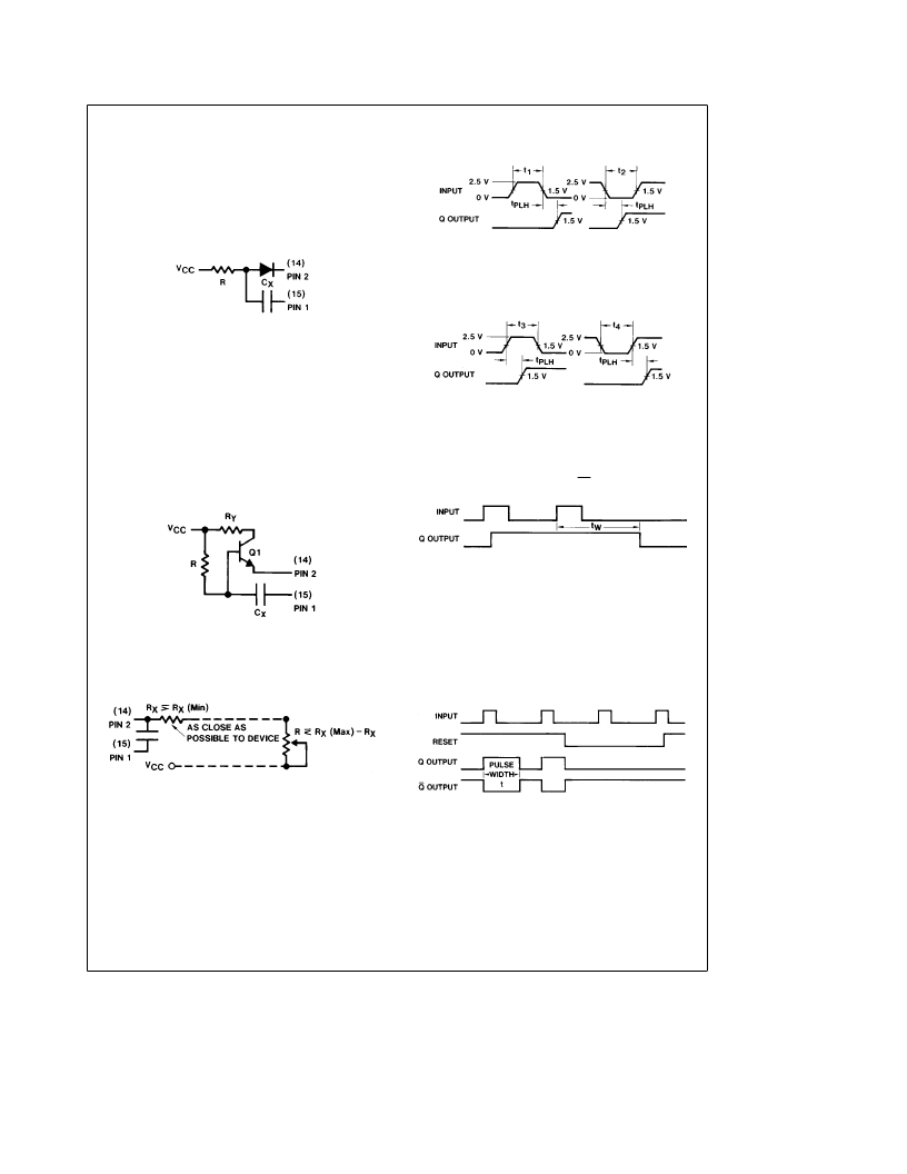
B. Use with high inverse leakage current electrolytic ca-
pacitors:
The diode in this configuration prevents high inverse
leakage currents through the capacitor by preventing
an inverse voltage across the capacitor. The use of
this configuration is not recommended with retriggera-
ble operation.
t
&
0.3 RC
X
TL/F/6611–5
C. Use to obtain extended pulse widths:
This configuration can be used to obtain extended
pulse widths, because of the larger timing resistor al-
lowed by beta multiplication. Electrolytics with high in-
verse leakage currents can be used.
R
k
R
X
(0.7) (h
FE
Q1) or
k
2.5 M
X
, whichever is the
lesser
R
X
(min)
k
R
Y
k
R
X
(5 k
X
s
R
Y
s
10 k
X
is recommended)
Q1: NPN silicon transistor with h
FE
requirements of
above equations, such as 2N5961 or 2N5962.
t
&
0.3 RC
X
TL/F/6611–6
This configuration is not recommended with retriggera-
ble operation.
5. To obtain variable pulse width by remote trimming, the
following circuit is recommended:
TL/F/6611–7
6. Under any operating condition, C
X
and R
X
(min) must be
kept as close to the circuit as possible to minimize stray
capacitance and reduce noise pickup.
7. Input Trigger Pulse Rules (See Triggering Truth Table)
TL/F/6611–8
Input to Pin 5(11),
Pin 4(12)
e
LOW
t
1
, t
3
e
Min. Positive Input Pulse Width
l
40 ns
t
2
, t
4
e
Min. Negative Input Pulse Width
l
40 ns
(Pin 3(13)
e
HIGH)
TL/F/6611–9
Input to Pin 4(12)
Pin 5(11)
e
HIGH
8. The retriggerable pulse width is calculated as shown be-
low:
(Pin 3(13)
e
HIGH)
t
W
e
t
a
t
PLH
e
K R
X
C
X
#
1
a
1
R
X
J
a
t
PLH
TL/F/6611–10
The retrigger pulse width is equal to the pulse width (t) plus a delay time. For
pulse widths greater than 500 ns, t
W
can be approximated as t. Retriggering will
not occur if the retrigger pulse comes within
&
0.3 C
X
(ns) after the initial trigger
pulse (i.e., during the discharge cycle).
9. Reset OperationDAn overriding clear (active LOW level)
is provided on each one shot. By applying a LOW to the
reset, any timing cycle can be terminated or any new cy-
cle inhibited until the LOW reset input is removed. Trigger
inputs will not produce spikes in the output when the re-
set is held LOW.
TL/F/6611–11
10. V
CC
and Ground wiring should conform to good high
frequency standards so that switching transients on V
CC
and Ground leads do not cause interaction between one
shots. Use of a 0.01 to 0.1
m
F bypass capacitor be-
tween V
CC
and Ground located near the DM9602 is rec-
ommended.
*
For further detailed device characteristics and output performance, please
refer to the NSC one-shot application note, AN-366.
4
相關(guān)PDF資料 |
PDF描述 |
|---|---|
| 9602FMQB | Dual Retriggerable, Resettable One Shots |
| 96050 | SORTIMENTSKOFFER LUFTFRACHTTAUGLICH L470 |
| 9609YEL | SWITCHSOCKET 16A YELLOW |
| 960JX | Microprocessor |
| 96101DC | Quad 2-input NAND Gate |
相關(guān)代理商/技術(shù)參數(shù) |
參數(shù)描述 |
|---|---|
| 9602FMQB | 制造商:NSC 制造商全稱:National Semiconductor 功能描述:Dual Retriggerable, Resettable One Shots |
| 96-02-L4 | 制造商:Misc 功能描述: |
| 96-02-M3 | 制造商:Misc 功能描述: |
| 9602M39P02 | 制造商: 功能描述: 制造商:undefined 功能描述: |
| 96-02-M4 | 制造商:Misc 功能描述: |
發(fā)布緊急采購,3分鐘左右您將得到回復(fù)。