- 您現(xiàn)在的位置:買賣IC網(wǎng) > PDF目錄360619 > 93LC66B 4K 2.5V Microwire Serial EEPROM PDF資料下載
參數(shù)資料
| 型號: | 93LC66B |
| 英文描述: | 4K 2.5V Microwire Serial EEPROM |
| 中文描述: | 4K的2.5V的微型導(dǎo)線串行EEPROM |
| 文件頁數(shù): | 2/12頁 |
| 文件大小: | 185K |
| 代理商: | 93LC66B |
93LC66A/B
DS21209A-page 2
Preliminary
1997 Microchip Technology Inc.
1.0
ELECTRICAL
CHARACTERISTICS
1.1
Maximum Ratings*
Vcc...................................................................................7.0V
All inputs and outputs w.r.t. Vss ................-0.6V to Vcc +1.0V
Storage temperature .....................................-65
Ambient temp. with power applied.................-65
Soldering temperature of leads (10 seconds).............+300
ESD protection on all pins................................................4 kV
°
°
C to +150
C to +125
°
°
°
C
C
C
*Notice:
cause permanent damage to the device. This is a stress rating only and
functional operation of the device at those or any other conditions
above those indicated in the operational listings of this specification is
not implied. Exposure to maximum rating conditions for extended peri-
ods may affect device reliability.
Stresses above those listed under “Maximum ratings” may
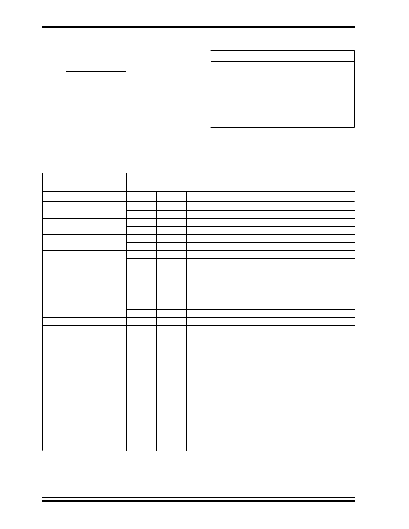
TABLE 1-1
PIN FUNCTION TABLE
Name
Function
CS
CLK
DI
DO
V
SS
NC
V
CC
Chip Select
Serial Data Clock
Serial Data Input
Serial Data Output
Ground
No Connect
Power Supply
TABLE 1-2
DC AND AC ELECTRICAL CHARACTERISTICS
All parameters apply over the specified
operating ranges unless otherwise
noted
Commercial (C):
Industrial (I):
V
V
CC
CC
= +2.5V to +6.0V
= +2.5V to +6.0V
Tamb = 0
Tamb = -40
°
C to +70
°
C to +85
°
C
°
C
Parameter
Symbol
Min.
Max.
Units
Conditions
High level input voltage
V
IH
1
2.0
Vcc +1
V
2.7V
≤
V
CC
≤
5.5V (Note 2)
V
IH
2
0.7 V
CC
Vcc +1
V
V
CC
< 2.7V
Low level input voltage
V
IL
1
-0.3
0.8
V
V
CC
> 2.7V (Note 2)
V
IL
2
-0.3
0.2 Vcc
V
V
CC
< 2.7V
Low level output voltage
V
OL
1
—
0.4
V
I
OL
= 2.1
μ
μ
A; Vcc = 4.5V
V
OL
2
—
0.2
V
I
OL
=100
A; Vcc = Vcc Min.
μ
A; Vcc = 4.5V
= -100
μ
A; Vcc = Vcc Min.
= V
SS
to V
CC
High level output voltage
V
OH
1
2.4
—
V
I
OH
= -400
V
OH
2
V
CC
-0.2
—
V
μ
μ
I
OH
Input leakage current
I
LI
-10
10
A
V
IN
Output leakage current
I
LO
-10
10
A
V
OUT
= V
SS
to V
CC
Pin capacitance
(all inputs/outputs)
C
IN
, C
OUT
—
7
pF
V
Tamb = +25
IN
/V
OUT
= 0 V (Notes 1 & 2)
°
C, F
CLK
= 2 MHz; Vcc = 6.0V
CLK
= 1 MHz; Vcc = 3.0V
= 1 MHz
Operating current
I
CC
read
—
1
500
mA
μ
A
mA
μ
A
MHz
MHz
F
F
CLK
I
CC
write
—
1.5
Standby current
I
CCS
—
1
CS = Vss
Clock frequency
F
CLK
—
2
1
V
V
CC
CC
> 4.5V
< 4.5V
Clock high time
T
CKH
250
—
ns
Clock low time
T
CKL
250
—
ns
Chip select setup time
T
CSS
50
—
ns
Relative to CLK
Chip select hold time
T
CSH
0
—
ns
Relative to CLK
Chip select low time
T
CSL
250
—
ns
Data input setup time
T
DIS
100
—
ns
Relative to CLK
Data input hold time
T
DIH
100
—
ns
Relative to CLK
Data output delay time
T
PD
—
400
ns
C
L
= 100 pF
Data output disable time
T
CZ
—
100
ns
C
L
= 100 pF (Note 2)
Status valid time
T
SV
—
500
ns
C
L
= 100 pF
Program cycle time
T
WC
—
6
ms
ERASE/WRITE mode
T
EC
—
6
ms
ERAL mode
T
WL
—
15
ms
WRAL mode
°
C, V
Endurance
—
1M
—
cycles
25
CC
= 5.0V, Block Mode (Note 3)
Note 1:
This parameter is tested at Tamb = 25
This parameter is periodically sampled and not 100% tested.
This application is not tested but guaranteed by characterization. For endurance estimates in a specific application, please consult the Total
Endurance Model which may be obtained on Microchip’s BBS or website.
°
C and Fclk = 1 MHz.
2:
3:
相關(guān)PDF資料 |
PDF描述 |
|---|---|
| 93LC66B | 4K 2.5V Microwire Serial EEPROM(4K位,2.5V,具上掉電數(shù)據(jù)保護(hù)電路,Microwire接口EEPROM) |
| 93LC66A | 4K 2.5V Microwire Serial EEPROM(4K位,2.5V,具上掉電數(shù)據(jù)保護(hù)電路,Microwire接口EEPROM) |
| 93LC66 | 4K 2.0V CMOS Serial EEPROM(4K位,2.0V,具上掉電數(shù)據(jù)保護(hù)電路,EEPROM) |
| 93LC46 | 1K 2.0V CMOS Serial EEPROM(1K位,2.0V,具上掉電數(shù)據(jù)保護(hù)電路,EEPROM) |
| 93LC56 | 2K 2.0V CMOS Serial EEPROM(2K位,2.0V,具上掉電數(shù)據(jù)保護(hù)電路,EEPROM) |
相關(guān)代理商/技術(shù)參數(shù) |
參數(shù)描述 |
|---|---|
| 93LC66B/P | 功能描述:電可擦除可編程只讀存儲器 256x16 RoHS:否 制造商:Atmel 存儲容量:2 Kbit 組織:256 B x 8 數(shù)據(jù)保留:100 yr 最大時鐘頻率:1000 KHz 最大工作電流:6 uA 工作電源電壓:1.7 V to 5.5 V 最大工作溫度:+ 85 C 安裝風(fēng)格:SMD/SMT 封裝 / 箱體:SOIC-8 |
| 93LC66B-/P | 制造商:Microchip Technology 功能描述:4k(256~16) 2MHz 2.5V to 5.5V VA / Microwire 8DIP 制造商:Microchip Technology 功能描述:4k(256~16) 2MHz 2.5V to 5.5V VA / Microwire 8DIP Bulk |
| 93LC66B/P | 制造商:Microchip Technology Inc 功能描述:IC EEPROM SERIAL 4K 93LC66 DIP8 |
| 93LC66B/SN | 功能描述:電可擦除可編程只讀存儲器 256x16 RoHS:否 制造商:Atmel 存儲容量:2 Kbit 組織:256 B x 8 數(shù)據(jù)保留:100 yr 最大時鐘頻率:1000 KHz 最大工作電流:6 uA 工作電源電壓:1.7 V to 5.5 V 最大工作溫度:+ 85 C 安裝風(fēng)格:SMD/SMT 封裝 / 箱體:SOIC-8 |
| 93LC66B/SN | 制造商:Microchip Technology Inc 功能描述:IC EEPROM SERIAL 4K 93LC66 SOIC8 |
發(fā)布緊急采購,3分鐘左右您將得到回復(fù)。