- 您現(xiàn)在的位置:買賣IC網(wǎng) > PDF目錄42387 > 93C46T-I/MS 64 X 16 MICROWIRE BUS SERIAL EEPROM, PDSO8 PDF資料下載
參數(shù)資料
| 型號: | 93C46T-I/MS |
| 元件分類: | PROM |
| 英文描述: | 64 X 16 MICROWIRE BUS SERIAL EEPROM, PDSO8 |
| 封裝: | PLASTIC, MSOP-8 |
| 文件頁數(shù): | 20/20頁 |
| 文件大?。?/td> | 510K |
| 代理商: | 93C46T-I/MS |
2002 Microchip Technology Inc.
DS21749A-page 9
93XX46, 93XX46A/B
2.8
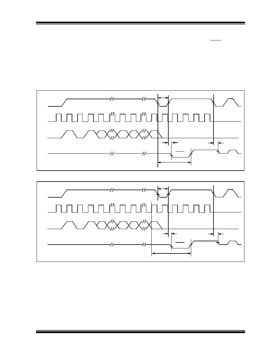
WRITE
The WRITE instruction is followed by 8 bits (If ORG is
low or A-version parts) or 16 bits (If ORG pin is high or
B-version devices) of data which are written into the
specified address. After the last data bit is put on the DI
pin, the falling edge of CS initiates the self-timed auto-
erase and programming cycle, except on ‘C’ devices
where the rising edge of CLK before the last data bit
initiates the write cycle.
The DO pin indicates the READY/BUSY status of the
device, if CS is brought high after a minimum of 250 ns
low (T
CSL). DO at logical “0” indicates that program-
ming is still in progress. DO at logical “1” indicates that
the register at the specified address has been written
with the data specified and the device is ready for
another instruction.
FIGURE 2-8:
WRITE TIMING FOR 93AA AND 93LC DEVICES
FIGURE 2-9:
WRITE TIMING FOR 93C DEVICES
CS
CLK
DI
DO
1
0
1
An
A0
Dx
D0
BUSY
READY
HIGH-Z
Twc
T
CSL
T
CZ
T
SV
CS
CLK
DI
DO
1
0
1
An
A0
Dx
D0
BUSY
READY
HIGH-Z
Twc
T
CSL
T
CZ
T
SV
發(fā)布緊急采購,3分鐘左右您將得到回復(fù)。