- 您現(xiàn)在的位置:買賣IC網(wǎng) > PDF目錄24825 > 935267386112 (NXP SEMICONDUCTORS) ALVC/VCX/A SERIES, 20 1-BIT DRIVER, TRUE OUTPUT, PDSO56 PDF資料下載
參數(shù)資料
| 型號(hào): | 935267386112 |
| 廠商: | NXP SEMICONDUCTORS |
| 元件分類: | 總線收發(fā)器 |
| 英文描述: | ALVC/VCX/A SERIES, 20 1-BIT DRIVER, TRUE OUTPUT, PDSO56 |
| 封裝: | 6.10 MM, PLASTIC, MO-153, SOT-364-1, TSSOP-56 |
| 文件頁(yè)數(shù): | 3/10頁(yè) |
| 文件大小: | 93K |
| 代理商: | 935267386112 |

December 1990
2
Philips Semiconductors
Product specication
8-bit parallel-in/serial-out shift register
74HC/HCT165
FEATURES
Asynchronous 8-bit parallel load
Synchronous serial input
Output capability: standard
ICC category: MSI
GENERAL DESCRIPTION
The 74HC/HCT165 are high-speed Si-gate CMOS devices
and are pin compatible with low power Schottky TTL
(LSTTL). They are specified in compliance with JEDEC
standard no. 7A.
The 74HC/HCT165 are 8-bit parallel-load or serial-in shift
registers with complementary serial outputs (Q7 and
Q7) available from the last stage. When the parallel load
(PL) input is LOW, parallel data from the D0 to
D7 inputs are loaded into the register asynchronously.
When PL is HIGH, data enters the register serially at the
Ds input and shifts one place to the right
(Q0 → Q1 → Q2, etc.) with each positive-going clock
transition. This feature allows parallel-to-serial converter
expansion by tying the Q7 output to the DS input of the
succeeding stage.
The clock input is a gated-OR structure which allows one
input to be used as an active LOW clock enable (CE) input.
The pin assignment for the CP and CE inputs is arbitrary
and can be reversed for layout convenience. The
LOW-to-HIGH transition of input CE should only take
place while CP HIGH for predictable operation. Either the
CP or the CE should be HIGH before the
LOW-to-HIGH transition of PL to prevent shifting the data
when PL is activated.
APPLICATIONS
Parallel-to-serial data conversion
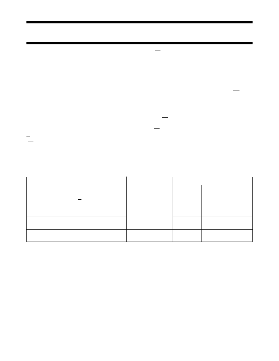
QUICK REFERENCE DATA
GND = 0 V; Tamb = 25 °C; tr = tf = 6 ns
Notes
1. CPD is used to determine the dynamic power dissipation (PD in W):
PD = CPD × VCC2 × fi +∑ (CL × VCC2 × fo) where:
fi = input frequency in MHz
fo = output frequency in MHz
∑ (CL × VCC2 × fo) = sum of outputs
CL = output load capacitance in pF
VCC = supply voltage in V
2. For HC the condition is VI = GND to VCC
For HCT the condition is VI = GND to VCC 1.5 V
ORDERING INFORMATION
See
“74HC/HCT/HCU/HCMOS Logic Package Information”.
SYMBOL
PARAMETER
CONDITIONS
TYPICAL
UNIT
HC
HCT
tPHL/ tPLH
propagation delay
CP to Q7, Q7
PL to Q7, Q7
D7 to Q7, Q7
CL = 15 pF; VCC = 5 V
16
15
11
14
17
11
ns
fmax
maximum clock frequency
56
48
MHz
CI
input capacitance
3.5
pF
CPD
power dissipation capacitance per
package
notes 1 and 2
35
pF
相關(guān)PDF資料 |
PDF描述 |
|---|---|
| 935267419551 | 1 CHANNEL(S), 1M bps, SERIAL COMM CONTROLLER, PQFP44 |
| 935267418529 | 1 CHANNEL(S), 1M bps, SERIAL COMM CONTROLLER, PQCC44 |
| 935267418512 | 1 CHANNEL(S), 1M bps, SERIAL COMM CONTROLLER, PQCC44 |
| 935267419557 | 1 CHANNEL(S), 1M bps, SERIAL COMM CONTROLLER, PQFP44 |
| 08-M150-KIT-FEC | IMPACT PRINTER KIT |
相關(guān)代理商/技術(shù)參數(shù) |
參數(shù)描述 |
|---|---|
| 935268081112 | 制造商:NXP Semiconductors 功能描述:SUB ONLY IC |
| 935268721125 | 制造商:NXP Semiconductors 功能描述:Buffer/Line Driver 1-CH Non-Inverting 3-ST CMOS 5-Pin TSSOP T/R |
| 935269304128 | 制造商:ST-Ericsson 功能描述:IC AUDIO CODEC W/TCH SCRN 48LQFP |
| 935269544557 | 制造商:NXP Semiconductors 功能描述:SUB ONLY TDA9587-2US1-V1.3 |
| 935269987557 | 制造商:NXP Semiconductors 功能描述:SUB ONLY TDA9587-1US1-V1.8 SUBBED TO 935269987557 |
發(fā)布緊急采購(gòu),3分鐘左右您將得到回復(fù)。