- 您現(xiàn)在的位置:買賣IC網(wǎng) > PDF目錄24813 > 935264167112 (NXP SEMICONDUCTORS) LVT SERIES, 16 1-BIT DRIVER, TRUE OUTPUT, PDSO48 PDF資料下載
參數(shù)資料
| 型號: | 935264167112 |
| 廠商: | NXP SEMICONDUCTORS |
| 元件分類: | 總線收發(fā)器 |
| 英文描述: | LVT SERIES, 16 1-BIT DRIVER, TRUE OUTPUT, PDSO48 |
| 封裝: | 6.10 MM, PLASTIC, MO-153ED, SOT-362-1, TSSOP-48 |
| 文件頁數(shù): | 9/12頁 |
| 文件大小: | 120K |
| 代理商: | 935264167112 |

Philips Semiconductors
Product specification
74LVT162374
3.3V 16-bit edge-triggered D-type flip-flop with
30
termination resistors (3-State)
1999 Sep 23
6
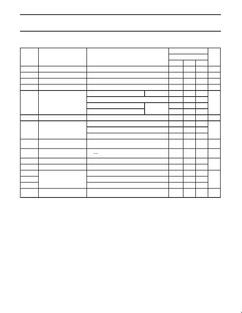
DC ELECTRICAL CHARACTERISTICS
LIMITS
SYMBOL
PARAMETER
TEST CONDITIONS
Temp = -40
°C to +85°C
UNIT
MIN
TYP1
MAX
VIK
Input clamp voltage
VCC = 2.7 V; IIK = –18 mA
–0.85
–1.2
V
VOH
High-level output voltage
VCC = 3.0 V; IOH = –12 mA
2.0
VOL
Low-level output voltage
VCC = 3.0 V; IOL = 12 mA
0.8
V
VRST
Power-up output Low voltage5
VCC = 3.6 V; IO = 1 mA; VI = GND or VCC
0.1
0.55
V
VCC = 3.6 V; VI = VCC or GND
Control pins
0.1
±1
I
Input leakage current
VCC = 0 or 3.6 V; VI = 5.5 V
0.4
10
A
II
Input leakage current
VCC = 3.6 V; VI = VCC
Data pins4
0.1
1
A
VCC = 3.6 V; VI = 0 V
Data pins4
–0.4
–5
IOFF
Output off current
VCC = 0 V; VI or VO = 0 to 4.5 V
0.1
±100
A
7
VCC = 3 V; VI = 0.8 V
75
135
IHOLD
Bus Hold current D inputs7
VCC = 3 V; VI = 2.0 V
–75
–135
A
VCC = 0 V to 3.6 V; VCC = 3.6 V
±500
IEX
Current into an output in the
High state when VO > VCC
VO = 5.5 V; VCC = 3.0 V
50
125
A
IPU/PD
Power up/down 3-State output
current3
VCC ≤ 1.2 V; VO = 0.5 V to VCC; VI = GND or VCC;
OE/OE = Don’t care
1
±100
A
IOZH
3-State output High current
VCC = 3.6 V; VO = 3.0 V; VI = VIH or VIL
0.5
5
A
IOZL
3-State output Low current
VCC = 3.6 V; VO = 0.5 V; VI = VIH or VIL
0.5
–5
A
ICCH
VCC = 3.6 V; Outputs High, VI = GND or VCC, IO = 0
0.07
0.12
ICCL
Quiescent supply current
VCC = 3.6 V; Outputs Low, VI = GND or VCC, IO = 0
4
6
mA
ICCZ
VCC = 3.6 V; Outputs Disabled; VI = GND or VCC, IO = 06
0.07
0.12
ICC
Additional supply current per
input pin2
VCC = 3 V to 3.6 V; One input at VCC-0.6 V,
Other inputs at VCC or GND
0.1
0.2
mA
NOTES:
1. All typical values are at VCC = 3.3 V and Tamb = 25°C.
2. This is the increase in supply current for each input at the specified voltage level other than VCC or GND
3. This parameter is valid for any VCC between 0V and 1.2V with a transition time of up to 10 msec. From VCC = 1.2 V to VCC = 3.3 V ± 0.3 V a
transition time of 100
sec is permitted. This parameter is valid for Tamb = 25°C only.
4. Unused pins at VCC or GND.
5. For valid test results, data must not be loaded into the flip-flops (or latches) after applying power.
6. ICCZ is measured with outputs pulled to VCC or GND.
7. This is the bus hold overdrive current required to force the input to the opposite logic state.
相關(guān)PDF資料 |
PDF描述 |
|---|---|
| 935264166112 | LVT SERIES, 16 1-BIT DRIVER, TRUE OUTPUT, PDSO48 |
| 935264166118 | LVT SERIES, 16 1-BIT DRIVER, TRUE OUTPUT, PDSO48 |
| 935264184112 | AHCT/VHCT SERIES, 8-INPUT NAND GATE, PDSO14 |
| 935264185118 | AHCT/VHCT SERIES, 8-INPUT NAND GATE, PDSO14 |
| 935264185112 | AHCT/VHCT SERIES, 8-INPUT NAND GATE, PDSO14 |
相關(guān)代理商/技術(shù)參數(shù) |
參數(shù)描述 |
|---|---|
| 935264217557 | 制造商:NXP Semiconductors 功能描述:SUB ONLY IC |
| 935267356112 | 制造商:NXP Semiconductors 功能描述:IC TEA1507PN |
| 935268081112 | 制造商:NXP Semiconductors 功能描述:SUB ONLY IC |
| 935268721125 | 制造商:NXP Semiconductors 功能描述:Buffer/Line Driver 1-CH Non-Inverting 3-ST CMOS 5-Pin TSSOP T/R |
| 935269304128 | 制造商:ST-Ericsson 功能描述:IC AUDIO CODEC W/TCH SCRN 48LQFP |
發(fā)布緊急采購,3分鐘左右您將得到回復(fù)。