- 您現(xiàn)在的位置:買(mǎi)賣(mài)IC網(wǎng) > PDF目錄36330 > 935163070112 (NXP SEMICONDUCTORS) COLOR SIGNAL ENCODER, PDIP32 PDF資料下載
參數(shù)資料
| 型號(hào): | 935163070112 |
| 廠(chǎng)商: | NXP SEMICONDUCTORS |
| 元件分類(lèi): | 顏色信號(hào)轉(zhuǎn)換 |
| 英文描述: | COLOR SIGNAL ENCODER, PDIP32 |
| 封裝: | 0.400 INCH, SHRINK, PLASTIC, SOT-232-1, DIP-32 |
| 文件頁(yè)數(shù): | 29/34頁(yè) |
| 文件大小: | 500K |
| 代理商: | 935163070112 |
第1頁(yè)第2頁(yè)第3頁(yè)第4頁(yè)第5頁(yè)第6頁(yè)第7頁(yè)第8頁(yè)第9頁(yè)第10頁(yè)第11頁(yè)第12頁(yè)第13頁(yè)第14頁(yè)第15頁(yè)第16頁(yè)第17頁(yè)第18頁(yè)第19頁(yè)第20頁(yè)第21頁(yè)第22頁(yè)第23頁(yè)第24頁(yè)第25頁(yè)第26頁(yè)第27頁(yè)第28頁(yè)當(dāng)前第29頁(yè)第30頁(yè)第31頁(yè)第32頁(yè)第33頁(yè)第34頁(yè)
July 1994
4
Philips Semiconductors
Preliminary specication
SECAM encoder
TDA8505
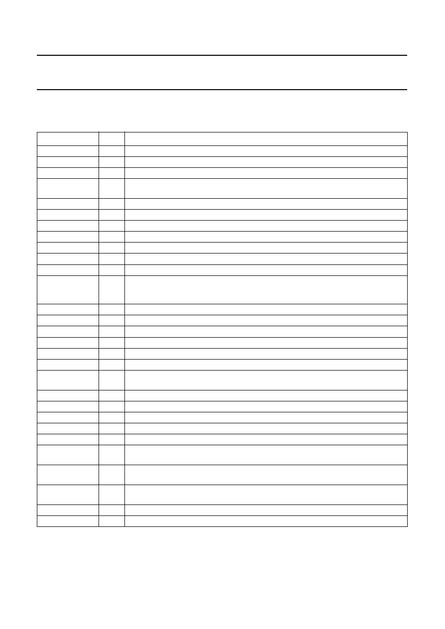
PINNING
D'R and D'B are the colour difference signals at the output of the multiplexer circuit; D'R =
1.9(RY) and
D'B = +1.5(B
Y), for an EBU bar of 75% the amplitudes are equal.
SYMBOL
PIN
DESCRIPTION
(RY)
1
colour difference input signal, for EBU bar of 75% 1.05 V (peak-to-peak value)
MCONTR
2
multiplexer control; input HIGH = RGB, input LOW =
(RY), (BY) and Y
(BY)
3
colour difference input signal, for EBU bar of 75% 1.33 V (peak-to-peak value)
FH/2
4
line pulse input divided-by-2 for synchronizing two or more encoders; when not used this
pin is connected to ground
Y
5
luminance input signal 1 V nominal without sync
TEST
6
test pin; must be connected to VCC (pin 8), or left open-circuit
R
7
RED input signal for EBU bar of 75% 0.7 V (peak-to-peak value)
VDDA
8
analog supply voltage for encoder part; 5 V nominal
G
9
GREEN input signal for EBU bar of 75% 0.7 V (peak-to-peak value)
VSSA
10
analog ground
B
11
BLUE input signal for EBU bar of 75% 0.7 V (peak-to-peak value)
Y/Y+SYNC
12
when this control input is LOW, Y without sync is connected to pin 5, input blanking at
pin 5 is active; when input is HIGH, Y+SYNC is connected to pin 5, input blanking at pin 5
is not active
LPFDR
13
modulator control loop lter output; black level of D'R = 4.40625 MHz
FADJ
14
adjustment pin for 4.286 MHz of HF pre-emphasis lter
LPFDB
15
modulator control loop lter output; black level of D'B = 4.250 MHz
FLT
16
lter tuning loop capacitor output
Vref
17
2.5 V internal reference voltage output
CHROMA
18
chrominance output, amplitude corresponds with Y+SYNC at the output of the delay line
Vext
19
external power supply for sandcastle generation; when not used this pin is connected to
ground
SAND
20
3-level sandcastle output pulse
CVBS
21
composite SECAM output 2 V (peak-to-peak value) nominal
NOTCH
22
Y+SYNC output after an internal resistor of 2 k
; a notch lter can be connected
Y+SYNC IN
23
Y+SYNC input, connected to the output of the delay line
LPF4.4
24
loop lter output for 4.40625 MHz reference oscillator
Y+SYNC OUT
25
Y+SYNC output, 2 V (peak-to-peak value) nominal, connected to the input of the
delay line
XTAL/PLL
VIDENT
26
control pin; input HIGH = crystal tuning, input LOW = PLL tuning, both without vertical
identication, 2.5 V = PLL tuning with vertical identication
VCO4.25
27
when used for PLL tuning a capacitor is connected; when used for crystal tuning a crystal
has to be connected (in series with a capacitor)
COLKIL
28
colour killing; input HIGH = active, internal colour difference signals are blanked
CS
29
composite sync input, 0.3 V (peak-to-peak value) nominal
相關(guān)PDF資料 |
PDF描述 |
|---|---|
| 935163360112 | 1-CHANNEL POWER SUPPLY SUPPORT CKT, PDSO8 |
| 935163320112 | 1-CHANNEL POWER SUPPLY SUPPORT CKT, PDSO8 |
| 935163350112 | 1-CHANNEL POWER SUPPLY SUPPORT CKT, PDSO8 |
| 935163280118 | 1-CHANNEL POWER SUPPLY SUPPORT CKT, PDSO8 |
| 935163280112 | 1-CHANNEL POWER SUPPLY SUPPORT CKT, PDSO8 |
相關(guān)代理商/技術(shù)參數(shù) |
參數(shù)描述 |
|---|---|
| 93516-PIX | 制造商:FCI 功能描述: |
| 93517-090001 | 制造商:FCI 功能描述:PCMCIA REV CARD FRAME 9P |
| 93517-150000 | 制造商:FCI 功能描述: |
| 93518097J | 制造商:Fiskars Brands Inc 功能描述:Fiskars 45mm Rotary Blades - Pinking (Fits Models 195800/154570/19680/19583) (Fr |
| 935181002005 | 功能描述:電容套件 HiTmpSilCap Kit 0402 1nF 10nF 33nF BD11V RoHS:否 制造商:Nichicon 電容范圍:10 uF to 680 uF 公差范圍: 電壓范圍:6.3 V to 25 V 產(chǎn)品:Aluminum Organic Polymer Capacitor Kit |
發(fā)布緊急采購(gòu),3分鐘左右您將得到回復(fù)。