- 您現(xiàn)在的位置:買賣IC網(wǎng) > PDF目錄24774 > 935084920112 (NXP SEMICONDUCTORS) TELEPHONE SPEECH CKT, PDSO20 PDF資料下載
參數(shù)資料
| 型號: | 935084920112 |
| 廠商: | NXP SEMICONDUCTORS |
| 元件分類: | 無繩電話/電話 |
| 英文描述: | TELEPHONE SPEECH CKT, PDSO20 |
| 封裝: | PLASTIC, SOT-163, SO-20 |
| 文件頁數(shù): | 6/38頁 |
| 文件大小: | 303K |
| 代理商: | 935084920112 |
第1頁第2頁第3頁第4頁第5頁當前第6頁第7頁第8頁第9頁第10頁第11頁第12頁第13頁第14頁第15頁第16頁第17頁第18頁第19頁第20頁第21頁第22頁第23頁第24頁第25頁第26頁第27頁第28頁第29頁第30頁第31頁第32頁第33頁第34頁第35頁第36頁第37頁第38頁

March 1994
14
Philips Semiconductors
Product specication
Low voltage versatile telephone transmission circuit
with dialler interface and transmit level dynamic limiting
TEA1064A
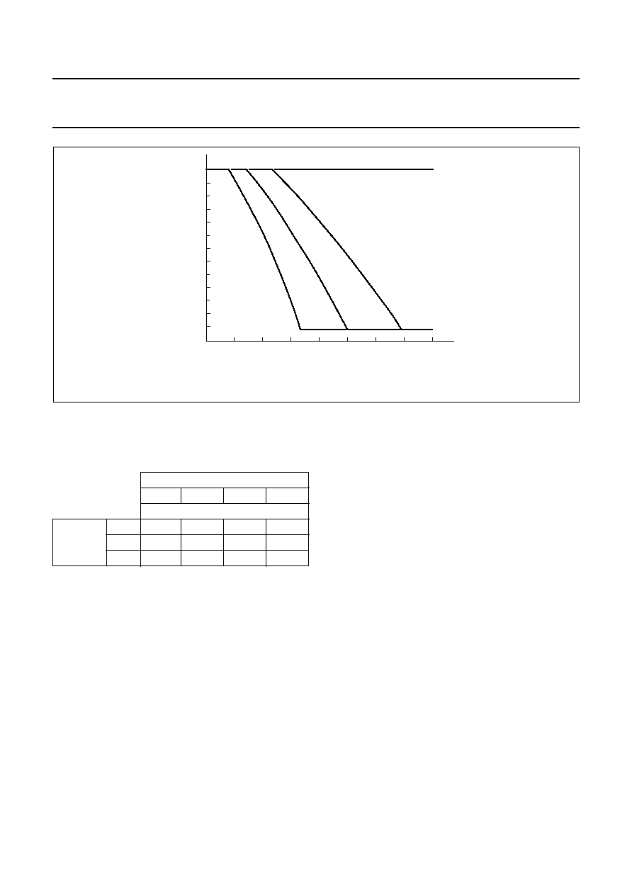
Fig.17 Variation of gain as a function of line current with R6 as a parameter; R9 = 20
.
handbook, full pagewidth
MGR072
6
5
4
3
2
1
0
Avd
(dB)
Iline (mA)
80
90
60
70
40
50
20
30
10
93.1 k
66.5 k
R6 =
∞
R6 =
118 k
Table 1
Values of R6 giving optimum line-loss
compensation at various values of exchange
supply voltage (Vexch) and exchange feeding
bridge resistance (Rexch); R9 = 20 .
MUTE input (see notes 1. and 2.)
MUTE = HIGH enables the DTMF input and inhibits the
microphone and receiving amplifier inputs.
MUTE = LOW or open-circuit disables the DTMF input and
enables the microphone and receiving amplifier inputs.
Switching MUTE gives negligible clicks at the telephone
outputs and on the line.
Dual-tone multi-frequency input DTMF (see note 1.)
When the DTMF input is enabled, dialling tones may be
sent on to the line. The voltage gain between DTMF-SLPE
and LN-VEE is typ. 26 dB less than the gain of the
microphone amplifier and varies with R7 in the same way
as the gain of the microphone amplifier. This means that
the tone level at the DTMF input has to be adjusted after
Rexch ()
400
600
800
1000
R6 (k
)
Vexch
(V)
36
84.5
66.5
X
48
118
93.1
77.8
66.5
60
X
97.6
84.5
setting the gain of the microphone amplifier. With
R7 =68k
the gain is typically 26 dB.
The signalling tones can be heard in the earpiece at a low
level (confidence tone).
Power-down input PD (see notes 1. and 2.)
During pulse dialling or register recall (timed loop break)
the telephone line is interrupted; as a consequence it
provides no supply for the transmission circuit connected
to VCC1 or for the peripherals between VCC2 and SLPE.
These supply gaps are bridged by the charges in the
capacitors C1 and C15. The requirements on these
capacitors are eased by applying a HIGH level to the PD
input during the time of the loop break. This reduces the
internal supply current ICC1 from (typ.) 1.3 mA to (typ.)
60
A and switches off the voltage regulator to prevent
discharge via LN and VCC2.
A HIGH level at PD also internally disconnects the
capacitor at REG so that the voltage stabilizer has no
switch-on delay after line interruptions. This minimizes the
contribution of the IC to the current waveform during pulse
dialling or register recall.
When the power-down facility is not required, the PD pin
can be left open-circuit or connected to SLPE.
Side-tone suppression
Suppression of the transmitted signal in the earpiece is
obtained by the anti-sidetone network comprising R1//Zline,
相關PDF資料 |
PDF描述 |
|---|---|
| 935084920118 | TELEPHONE SPEECH CKT, PDSO20 |
| 935084930112 | TELEPHONE SPEECH CKT, PDIP20 |
| 0672.400 | Circular Connector; MIL SPEC:MIL-C-26482, Series I, Solder; Body Material:Aluminum; Series:PT06; Number of Contacts:55; Connector Shell Size:22; Connecting Termination:Solder; Circular Shell Style:Straight Plug; Body Style:Straight |
| 0672.500 | Circular Connector; No. of Contacts:61; Series:; Body Material:Aluminum; Connecting Termination:Solder; Connector Shell Size:24; Circular Contact Gender:Pin; Circular Shell Style:Straight Plug; Insert Arrangement:24-61 |
| 935085450112 | F/FAST SERIES, DUAL POSITIVE EDGE TRIGGERED D FLIP-FLOP, COMPLEMENTARY OUTPUT, PDSO14 |
相關代理商/技術參數(shù) |
參數(shù)描述 |
|---|---|
| 935087-000 | 制造商:TE Connectivity 功能描述:301A511-51-05/164-0 - Bulk |
| 935087N001 | 制造商:TE Connectivity 功能描述:301A511-51-05/164-CS7092 制造商:TE Connectivity 功能描述:301A511-51-05/164-CS7092 - Bulk |
| 9350DC-200-0GZZZA | 制造商:Siemens 功能描述: |
| 9350DC-200-0ZZZTA | 制造商:Siemens 功能描述: |
| 9350DC-200-0ZZZZA | 制造商:Siemens 功能描述: |
發(fā)布緊急采購,3分鐘左右您將得到回復。