- 您現在的位置:買賣IC網 > PDF目錄24670 > 933897010112 (NXP SEMICONDUCTORS) SPECIALTY TELECOM CIRCUIT, PDIP8 PDF資料下載
參數資料
| 型號: | 933897010112 |
| 廠商: | NXP SEMICONDUCTORS |
| 元件分類: | 通信及網絡 |
| 英文描述: | SPECIALTY TELECOM CIRCUIT, PDIP8 |
| 封裝: | 0.300 INCH, PLASTIC, SOT-97, DIP-8 |
| 文件頁數: | 13/18頁 |
| 文件大小: | 144K |
| 代理商: | 933897010112 |
September 1994
4
Philips Semiconductors
Product specication
Supply circuit with power-down for
telephone set peripherals
TEA1081
FUNCTIONAL DESCRIPTION
The TEA1081 is a supply interface between telephone line
and peripheral devices in the telephone set. The high input
impedance of the circuit allows direct connection to the
telephone line (via a diode bridge). An inductor function is
obtained by amplifier A1, resistor RS (see Fig.1) and an
external low-pass RC filter.
Under the control of amplifier A2, transistor TR1 supplies
peripheral devices and transistor TR2 minimizes line
signal distortion by momentarily diverting input current to
ground whenever the instantaneous value of the line
voltage drops below the output voltage.
Internal circuits are biased by a temperature and line
voltage compensated reference current source.
The power-down circuit isolates the supply circuit from
external circuitry.
Line terminals: LN and VN (pins 1 and 2)
The input terminals LN and VN can be connected directly
to the line. The minimum DC line voltage required at the
input is expressed by formula (1); see also Table 1.
(1)
Table 1 Explanation of formula (1).
The internal current (IINT) at IO = 0 mA is typically 0.8 mA
at VLN = 4 V and reaches a maximum of 1.4 mA at
VLN =12V.
Supply terminals: QS and VA (pins 7 and 6)
Peripheral devices are supplied from QS (pin 7). Two
modes of output voltage regulation are available.
OUTPUT VOLTAGE FOLLOWS LINE VOLTAGE (SEE FIG.3)
The TEA1081 operates in this mode when there is no
external resistor (RV) between QS and VA (see Fig.6).
SYMBOL
DESCRIPTION
I1
input current
RS
internal series resistance
VLNmin
minimum instantaneous line voltage
(1.4 V at IO = 5 mA)
VLN(P)
required peak level of AC line voltage
V
LN
I
1
R
S
×
V
LNmin
V
LN P
() V
()
++
=
The output voltage follows the line voltage and is
expressed by formula (2); see also Table 2.
(2)
Table 2 Explanation of formula (2).
REGULATED OUTPUT VOLTAGE (SEE FIG.4)
The circuit operates in this mode when an external resistor
(RV) is connected between QS and VA (see Fig.6).
The output voltage is held constant at VO = 2 × I6 × RV (V)
as soon as the line voltage
VLN >(2 × I6 × RV +I1 × RS + 0.5) (V)
The control current I6 is typically 20
A.
SYMBOL
DESCRIPTION
VLN
line voltage
I1
input current
RS
internal series resistance
V
O
V
LN
I
1
R
S
0.5
+
×
()
–
V
()
=
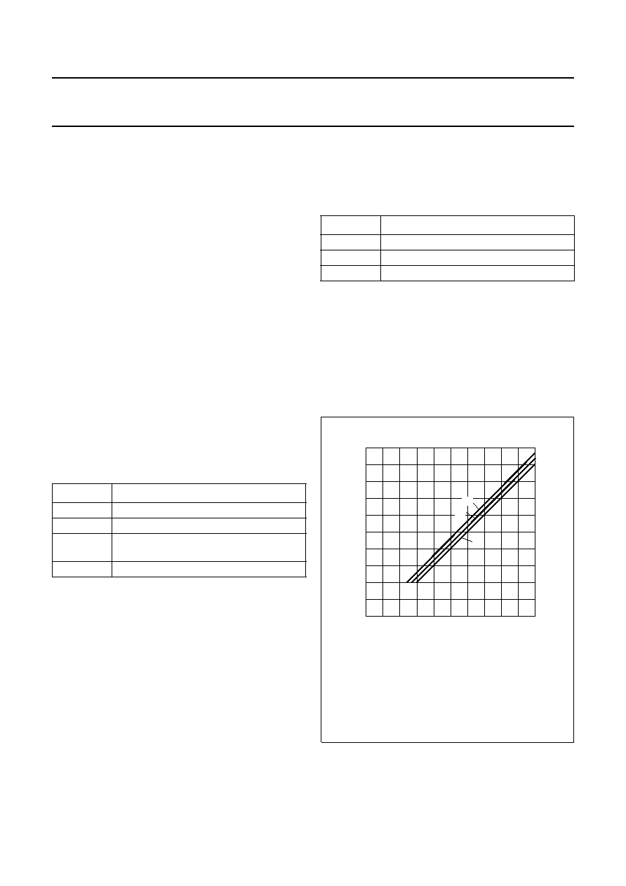
Fig.3 Output voltage as a function of line voltage.
Application without RV.
(1) I1 = 5 mA.
(2) I1 = 20 mA.
(3) I1 = 30 mA; not valid for TEA1081T.
handbook, halfpage
010
10
0
2
MLC168
4
6
8
24
6
8
VO
(V)
V
(V)
LN
(1)
(2)
(3)
相關PDF資料 |
PDF描述 |
|---|---|
| 933897020112 | SPECIALTY TELECOM CIRCUIT, PDSO8 |
| 933897020118 | SPECIALTY TELECOM CIRCUIT, PDSO8 |
| 0561250128 | COPPER ALLOY, TIN (120) FINISH, WIRE TERMINAL |
| 933897220115 | UHF BAND, Si, PNP, RF SMALL SIGNAL TRANSISTOR |
| 9339-10223 | POWER/SIGNAL RELAY, 3PST, MOMENTARY, 0.175A (COIL), 28VDC (COIL), 4900mW (COIL), 25A (CONTACT), 28VDC (CONTACT), PANEL MOUNT |
相關代理商/技術參數 |
參數描述 |
|---|---|
| 9338-A17R | 制造商:GC Electronics 功能描述: |
| 9338DMQB | 制造商:Rochester Electronics LLC 功能描述:- Bulk |
| 9338FMQB | 制造商:Rochester Electronics LLC 功能描述:- Bulk |
| 9338PC | 制造商:Rochester Electronics LLC 功能描述:- Bulk |
| 9338PCQR | 制造商:Rochester Electronics LLC 功能描述:- Bulk |
發(fā)布緊急采購,3分鐘左右您將得到回復。