- 您現(xiàn)在的位置:買賣IC網(wǎng) > PDF目錄24670 > 933865300118 (NXP SEMICONDUCTORS) LIQUID CRYSTAL DISPLAY DRIVER, PDSO40 PDF資料下載
參數(shù)資料
| 型號: | 933865300118 |
| 廠商: | NXP SEMICONDUCTORS |
| 元件分類: | 顯示驅(qū)動器 |
| 英文描述: | LIQUID CRYSTAL DISPLAY DRIVER, PDSO40 |
| 封裝: | PLASTIC, SOT-158-1, VSOP-40 |
| 文件頁數(shù): | 15/40頁 |
| 文件大小: | 243K |
| 代理商: | 933865300118 |
第1頁第2頁第3頁第4頁第5頁第6頁第7頁第8頁第9頁第10頁第11頁第12頁第13頁第14頁當(dāng)前第15頁第16頁第17頁第18頁第19頁第20頁第21頁第22頁第23頁第24頁第25頁第26頁第27頁第28頁第29頁第30頁第31頁第32頁第33頁第34頁第35頁第36頁第37頁第38頁第39頁第40頁
1998 May 04
22
Philips Semiconductors
Product specication
Universal LCD driver for low multiplex
rates
PCF8566
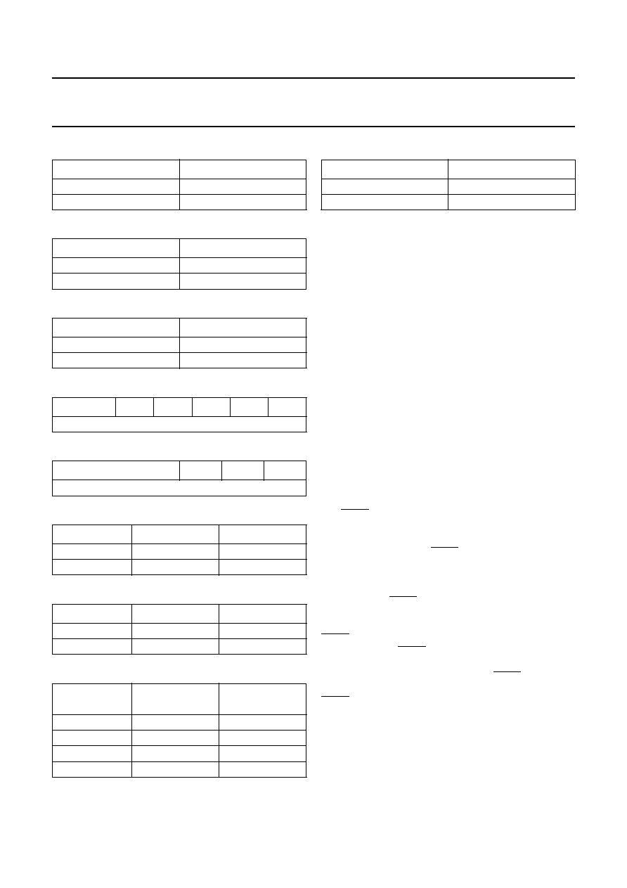
Table 7
LCD bias conguration
Table 8
Display status
Table 9
Power dissipation mode
Table 10 Load data pointer
Table 11 Device select
Table 12 Input bank selection
Table 13 Output bank selection
Table 14 Blinking frequency
LCD BIAS
BIT B
1
3bias
0
1
2bias
1
DISPLAY STATUS
BIT E
Disabled (blank)
0
Enabled
1
MODE
BIT LP
Normal mode
0
Power-saving mode
1
BITS
P4
P3
P2
P1
P0
5-bit binary value of 0 to 23
BITS
A0
A1
A2
3-bit binary value of 0 to 7
STATIC
1 : 2 MUX
BIT 1
RAM bit 0
RAM bits 0, 1
0
RAM bit 2
RAM bits 2, 3
1
STATIC
1 : 2 MUX
BIT 0
RAM bit 0
RAM bits 0, 1
0
RAM bit 2
RAM bits 2, 3
1
BLINK
FREQUENCY
BIT BF1
BIT BF0
Off
0
2Hz
0
1
1Hz
1
0
0.5 Hz
1
Table 15 Blink mode selection
7.9
Display controller
The display controller executes the commands identified
by the command decoder. It contains the status registers
of the PCF8566 and coordinates their effects.
The controller is also responsible for loading display data
into the display RAM as required by the filling order.
7.10
Cascaded operation
In large display configurations, up to 16 PCF8566s can be
distinguished on the same I2C-bus by using the 3-bit
hardware subaddress (A0, A1 and A2) and the
programmable I2C-bus slave address (SA0). It is also
possible to cascade up to 16 PCF8566s. When cascaded,
several PCF8566s are synchronized so that they can
share the backplane signals from one of the devices in the
cascade. Such an arrangement is cost-effective in large
LCD applications since the outputs of only one device
need to be through-plated to the backplane electrodes of
the display. The other PCF8566s of the cascade
contribute additional segment outputs but their backplane
outputs are left open-circuit (Fig.17).
The SYNC line is provided to maintain the correct
synchronization between all cascaded PCF8566s.
This synchronization is guaranteed after the power-on
reset. The only time that SYNC is likely to be needed is if
synchronization is accidentally lost (e.g. by noise in
adverse electrical environments; or by the definition of a
multiplex mode when PCF8566s with differing SA0 levels
are cascaded). SYNC is organized as an input/output pin;
the output section being realized as an open-drain driver
with an internal pull-up resistor. A PCF8566 asserts the
SYNC line at the onset of its last active backplane signal
and monitors the SYNC line at all other times.
Should synchronization in the cascade be lost, it will be
restored by the first PCF8566 to assert SYNC. The timing
relationships between the backplane waveforms and the
SYNC signal for the various drive modes of the PCF8576
are shown in Fig.18. The waveforms are identical with the
parent device PCF8576. Cascade ability between
PCF8566s and PCF8576s is possible, giving cost effective
LCD applications.
BLINK MODE
BIT A
Normal blinking
0
Alternation blinking
1
相關(guān)PDF資料 |
PDF描述 |
|---|---|
| 933865310112 | LIQUID CRYSTAL DISPLAY DRIVER, PDIP40 |
| 935263625026 | LIQUID CRYSTAL DISPLAY DRIVER, U |
| 0561168228 | PHOSPHOR BRONZE, TIN (40) FINISH, WIRE TERMINAL |
| 933876860602 | F/FAST SERIES, POSITIVE EDGE TRIGGERED D FLIP-FLOP, TRUE OUTPUT, PDIP16 |
| 933893120623 | F/FAST SERIES, POSITIVE EDGE TRIGGERED D FLIP-FLOP, TRUE OUTPUT, PDSO16 |
相關(guān)代理商/技術(shù)參數(shù) |
參數(shù)描述 |
|---|---|
| 933871-1 | 制造商:TE Connectivity 功能描述:GUIDE, MODIFIED - Bulk |
| 9-338728-0 | 功能描述:集管和線殼 MICROM. MOB SMD CON RoHS:否 產(chǎn)品種類:1.0MM Rectangular Connectors 產(chǎn)品類型:Headers - Pin Strip 系列:DF50 觸點類型:Pin (Male) 節(jié)距:1 mm 位置/觸點數(shù)量:16 排數(shù):1 安裝風(fēng)格:SMD/SMT 安裝角:Right 端接類型:Solder 外殼材料:Liquid Crystal Polymer (LCP) 觸點材料:Brass 觸點電鍍:Gold 制造商:Hirose Connector |
| 933873-1 | 制造商:TE Connectivity 功能描述:PLATE, CYL MTG. - Bulk |
| 933879-8 | 制造商:TE Connectivity 功能描述:WHEEL, WIRE SELECTOR - Bulk |
| 933879-9 | 制造商:TE Connectivity 功能描述:WHEEL, WIRE SELECTOR - Bulk |
發(fā)布緊急采購,3分鐘左右您將得到回復(fù)。