- 您現(xiàn)在的位置:買賣IC網(wǎng) > PDF目錄42368 > 933757470118 (NXP SEMICONDUCTORS) QUAD 1-CHANNEL, SGL POLE SGL THROW SWITCH, PDSO16 PDF資料下載
參數(shù)資料
| 型號: | 933757470118 |
| 廠商: | NXP SEMICONDUCTORS |
| 元件分類: | 多路復(fù)用及模擬開關(guān) |
| 英文描述: | QUAD 1-CHANNEL, SGL POLE SGL THROW SWITCH, PDSO16 |
| 封裝: | PLASTIC, SOT-109, SO-16 |
| 文件頁數(shù): | 8/15頁 |
| 文件大小: | 122K |
| 代理商: | 933757470118 |
September 1993
2
Philips Semiconductors
Product specication
Quad bilateral switches
74HC/HCT4316
FEATURES
Low “ON” resistance:
160
(typ.) at VCC VEE = 4.5 V
120
(typ.) at VCC VEE = 6.0 V
80
(typ.) at VCC VEE = 9.0 V
Logic level translation:
to enable 5 V logic to communicate
with
± 5 V analog signals
Typical “break before make” built in
Output capability: non-standard
ICC category: MSI
GENERAL DESCRIPTION
The 74HC/HCT4316 are high-speed Si-gate CMOS
devices. They are specified in compliance with JEDEC
standard no. 7A.
The 74HC/HCT4316 have four independent analog
switches. Each switch has two input/output terminals
(nY, nZ) and an active HIGH select input (nS). When the
enable input (E) is HIGH, all four analog switches are
turned off.
Current through a switch will not cause additional VCC
current provided the voltage at the terminals of the switch
is maintained within the supply voltage range;
VCC >> (VY, VZ) >> VEE. Inputs nY and nZ are electrically
equivalent terminals.
VCC and GND are the supply voltage pins for the digital
control inputs (E and nS). The VCC to GND ranges are 2.0
to 10.0 V for HC and 4.5 to 5.5 V for HCT.
The analog inputs/outputs (nY and nZ) can swing between
VCC as a positive limit and VEE as a negative limit.
VCC VEE may not exceed 10.0 V.
See the “4016” for the version without logic level
translation.
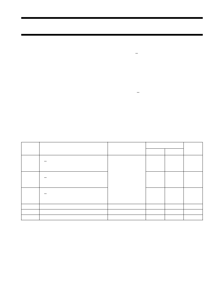
QUICK REFERENCE DATA
VEE = GND = 0 V; Tamb =25 °C; tr =tf = 6 ns
SYMBOL
PARAMETER
CONDITIONS
TYPICAL
UNIT
HC
HCT
tPZH
turn “ON” time
CL = 15 pF; RL =1 k;
VCC =5 V
E to VOS
19
ns
nS to VOS
16
17
ns
tPZL
turn “ON” time
E to VOS
19
24
ns
nS to VOS
16
21
ns
tPHZ/ tPLZ
turn “OFF” time
E to VOS
20
21
ns
nS to VOS
16
19
ns
CI
input capacitance
3.5
pF
CPD
power dissipation capacitance per switch
notes 1 and 2
13
14
pF
CS
max. switch capacitance
5
pF
Notes
1. CPD is used to determine the dynamic power
dissipation (PD in W):
PD =CPD × VCC2 × fi +∑ {(CL + CS) × VCC2 × fo }
where:
fi = input frequency in MHz
fo = output frequency in MHz
∑ {(CL + CS) × VCC2 × fo } = sum of outputs
CL = output load capacitance in pF
CS = max. switch capacitance in pF
VCC = supply voltage in V
2. For HC the condition is VI = GND to VCC
For HCT the condition is VI = GND to VCC 1.5 V
相關(guān)PDF資料 |
PDF描述 |
|---|---|
| 935188500112 | QUAD 1-CHANNEL, SGL POLE SGL THROW SWITCH, PDSO16 |
| 933757460112 | QUAD 1-CHANNEL, SGL POLE SGL THROW SWITCH, PDIP16 |
| 935186960118 | QUAD 1-CHANNEL, SGL POLE SGL THROW SWITCH, PDSO16 |
| 933825670005 | QUAD 1-CHANNEL, SGL POLE SGL THROW SWITCH, UUC |
| 933757440652 | QUAD 1-CHANNEL, SGL POLE SGL THROW SWITCH, PDIP16 |
相關(guān)代理商/技術(shù)參數(shù) |
參數(shù)描述 |
|---|---|
| 93378-003 | 制造商:FCI 功能描述:MEMORY CARD RECEPTACLE - Bulk |
| 9337-A17R | 制造商:GC Electronics 功能描述: |
| 9337C | 制造商:Hubbell Premise Wiring 功能描述: |
| 9337-CHR-100 | 制造商:Belden Inc 功能描述: |
| 9337CKE100M | 制造商:RFMD 制造商全稱:RF Micro Devices 功能描述:380W GaN WIDEBAND PULSED |
發(fā)布緊急采購,3分鐘左右您將得到回復(fù)。