- 您現(xiàn)在的位置:買賣IC網(wǎng) > PDF目錄24631 > 9309-01 (PEREGRINE SEMICONDUCTOR CORP) PRESCALER, CDSO8 PDF資料下載
參數(shù)資料
| 型號(hào): | 9309-01 |
| 廠商: | PEREGRINE SEMICONDUCTOR CORP |
| 元件分類: | 諧振器 |
| 英文描述: | PRESCALER, CDSO8 |
| 封裝: | CERAMIC, SOIC-8 |
| 文件頁數(shù): | 2/6頁 |
| 文件大?。?/td> | 219K |
| 代理商: | 9309-01 |
Product Specification
PE9309
Page 2 of 6
2007-2010 Peregrine Semiconductor Corp. All rights reserved.
Document No. 70-0241-05
│ UltraCMOS RFIC Solutions
Electrostatic Discharge (ESD) Precautions
When handling this UltraCMOS device, observe
the same precautions that you would use with other
ESD-sensitive devices. Although this device
contains circuitry to protect it from damage due to
ESD, precautions should be taken to avoid
exceeding the specified rating.
Latch-Up Avoidance
Unlike conventional CMOS devices, UltraCMOS
devices are immune to latch-up.
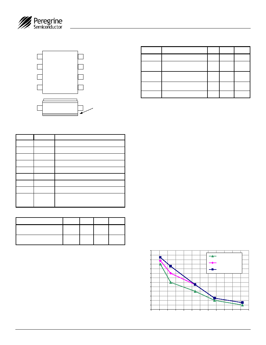
Figure 3. Pin Configuration (Top View)
Table 2. Pin Descriptions
Pin No.
Pin Name
Description
1
VBYPS
Prescaler Supply Bypass
2
VBYPS
Prescaler Supply Bypass
3
IN
RF Input
4
GND
Ground
5
NC
Not Connected
6
OUT
RF Output.
7
VDD
Supply Voltage
8
RBIAS
Frequency-Selecting Bias Resistor
GND
Bottom of the package is Ground.
Connecting the bottom of the package to
ground is required
Table 4. Absolute Maximum Ratings
Symbol
Parameter/Conditions
Min
Max
Units
VDD
DC Supply voltage
3.0
V
TST
Storage temperature
range
-65
150
°C
TOP
Operating temperature
range
-40
85
°C
VESD
ESD voltage (Human
Body Model)
250
V
PINMAX
Maximum input power
14
dBm
Device Functional Considerations
The PE9309 divides a 3.0 GHz to 13.5 GHz input
signal by four, producing a 750 MHz to 3.375 GHz
output signal. In order for the prescaler to work
properly, several conditions need to be adhered to.
It is crucial that pins 1, 2 and 7 be supplied with
bypass capacitors to ground. In addition, the output
signal (pins 6) needs to be ac coupled via an
external capacitor as shown in the test circuit in
Figure 5.
The input frequency range is selected by the value
of RBIAS according to Figure 4.
The ground pattern on the board should be made as
wide as possible to minimize ground impedance.
The bottom of the package is the primary ground
connection and it needs to be soldered to the PCB
ground.
Exceeding absolute maximum ratings may cause
permanent damage. Operation should be restricted
to the limits in the Operating Ranges table.
Operation between operating range maximum and
absolute maximum for extended periods may reduce
reliability.
9309
1
2
3
4
RF IN
GND
VBYPS
8
7
6
5
RBIAS
VDD
RF OUT
NC
VBYPS
Top View
Side View
GND
Parameter
Min
Typ
Max
Units
Supply Voltage (VDD)
2.45
2.6
2.75
V
Supply Current (IDD)
6
23
mA
Table 3. Operating Ranges
Figure 4. Frequency versus RBIAS
2
3
4
5
6
7
8
9
10
11
12
13
14
15
0
5
10
15
20
25
30
35
40
45
50
55
60
RBIAS (KOhm)
F
req
ue
nc
y(
G
H
z)
Lower Freq Lim
Optimal Freq Lim
Upper Freq Lim
相關(guān)PDF資料 |
PDF描述 |
|---|---|
| 930920 | BARRIER STRIP TERMINAL BLOCK |
| 930920-G30 | BARRIER STRIP TERMINAL BLOCK |
| 930919 | BARRIER STRIP TERMINAL BLOCK |
| 930919-G30 | BARRIER STRIP TERMINAL BLOCK |
| 930917 | BARRIER STRIP TERMINAL BLOCK |
相關(guān)代理商/技術(shù)參數(shù) |
參數(shù)描述 |
|---|---|
| 930903 | 制造商:MOLEX 制造商全稱:Molex Electronics Ltd. 功能描述:3.81mm (.150") Pitch Beau? EuroMate? Pluggable PCB Terminal Block, Dual Level, 270° Wire Entry, 3 Circuits |
| 930904 | 制造商:MOLEX 制造商全稱:Molex Electronics Ltd. 功能描述:3.81mm (.150") Pitch Beau? EuroMate? Pluggable PCB Terminal Block, Dual Level, 270° Wire Entry, 4 Circuits |
| 930905 | 制造商:MOLEX 制造商全稱:Molex Electronics Ltd. 功能描述:3.81mm (.150") Pitch Beau? EuroMate? Pluggable PCB Terminal Block, Dual Level, 270° Wire Entry, 5 Circuits |
| 930906 | 制造商:MOLEX 制造商全稱:Molex Electronics Ltd. 功能描述:3.81mm (.150") Pitch Beau? EuroMate? Pluggable PCB Terminal Block, Dual Level, 270° Wire Entry, 6 Circuits |
| 930907 | 制造商:MOLEX 制造商全稱:Molex Electronics Ltd. 功能描述:3.81mm (.150") Pitch Beau? EuroMate? Pluggable PCB Terminal Block, Dual Level, 270° Wire Entry, 7 Circuits |
發(fā)布緊急采購,3分鐘左右您將得到回復(fù)。