- 您現(xiàn)在的位置:買賣IC網(wǎng) > PDF目錄24631 > 930400802 (ATMEL CORP) FPGA, 2304 CLBS, 40000 GATES, PQFP256 PDF資料下載
參數(shù)資料
| 型號: | 930400802 |
| 廠商: | ATMEL CORP |
| 元件分類: | FPGA |
| 英文描述: | FPGA, 2304 CLBS, 40000 GATES, PQFP256 |
| 封裝: | MQFPF-256 |
| 文件頁數(shù): | 12/43頁 |
| 文件大小: | 673K |
| 代理商: | 930400802 |
第1頁第2頁第3頁第4頁第5頁第6頁第7頁第8頁第9頁第10頁第11頁當(dāng)前第12頁第13頁第14頁第15頁第16頁第17頁第18頁第19頁第20頁第21頁第22頁第23頁第24頁第25頁第26頁第27頁第28頁第29頁第30頁第31頁第32頁第33頁第34頁第35頁第36頁第37頁第38頁第39頁第40頁第41頁第42頁第43頁
2
AT40KEL040
4155H–AERO–02/06
***
Note:
1. Packages with FCK will have 8 less clocks.
Description
The AT40KEL040 is a fully PCI-compliant, SRAM-based FPGA with distributed 18 ns
programmable synchronous/asynchronous, dual port/single port SRAM, 8 global clocks,
Cache Logic ability (partially or fully reconfigurable without loss of data), automatic com-
ponent generators, and 50,000 usable gates. I/O counts range from 128 to 384 in Aero-
space standard packages and support 3.3V.
The AT40KEL040 is designed to quickly implement high performance, large gate count
designs through the use of synthesis and schematic-based tools used on a PC and
Sun platform. Atmel’s design tools provide seamless integration with industry standard
tools such as Synplicity, Modelsim, Exemplar and Viewlogic. See the IDS datasheet for
other supported tools.
The AT40KEL040 can be used as a co-processor for high-speed (DSP/processor-
based) designs by implementing a variety of compute-intensive, arithmetic functions.
These include adaptive finite impulse response (FIR) filters, Fast Fourier Transforms
(FFT), convolvers, interpolators and discrete-cosine transforms (DCT) that are required
for video compression and decompression, encryption, convolution and other multime-
dia applications.
Fast, Flexible and
Efficient SRAM
The AT40KEL040 FPGA offers a patented distributed 11 - 13 ns SRAM capability where
the RAM can be used without losing logic resources. Multiple independent, synchronous
or asynchronous, dual port or single port RAM functions (FIFO, scratch pad, etc.) can be
created using Atmel’s macro generator tool.
Fast, Efficient Array and
Vector Multipliers
The AT40KEL040’s patented 8-sided core cell with direct horizontal, vertical and diago-
nal cell-to-cell connections implements ultra fast array multipliers without using any bus-
ing resources. The AT40KEL040’s Cache Logic capability enables a large number of
design coefficients and variables to be implemented in a very small amount of silicon,
enabling vast improvement in system speed at much lower cost than conventional
FPGAs.
Cache Logic Design
The AT40KEL040 is capable of implementing Cache Logic (Dynamic full/partial logic
reconfiguration, without loss of data, on-the-fly) for building adaptive logic and systems.
As new logic functions are required, they can be loaded into the logic cache without los-
ing the data already there or disrupting the operation of the rest of the chip; replacing or
complementing the active logic. The AT40KEL040 can act as a reconfigurable co-pro-
cessor.
Automatic Component
Generators
The AT40KEL040 FPGA family is capable of implementing user-defined, automatically
generated, macros in multiple designs; speed and functionality are unaffected by the
macro orientation or density of the target device. This enables the fastest, most predict-
able and efficient FPGA design approach and minimizes design risk by reusing already
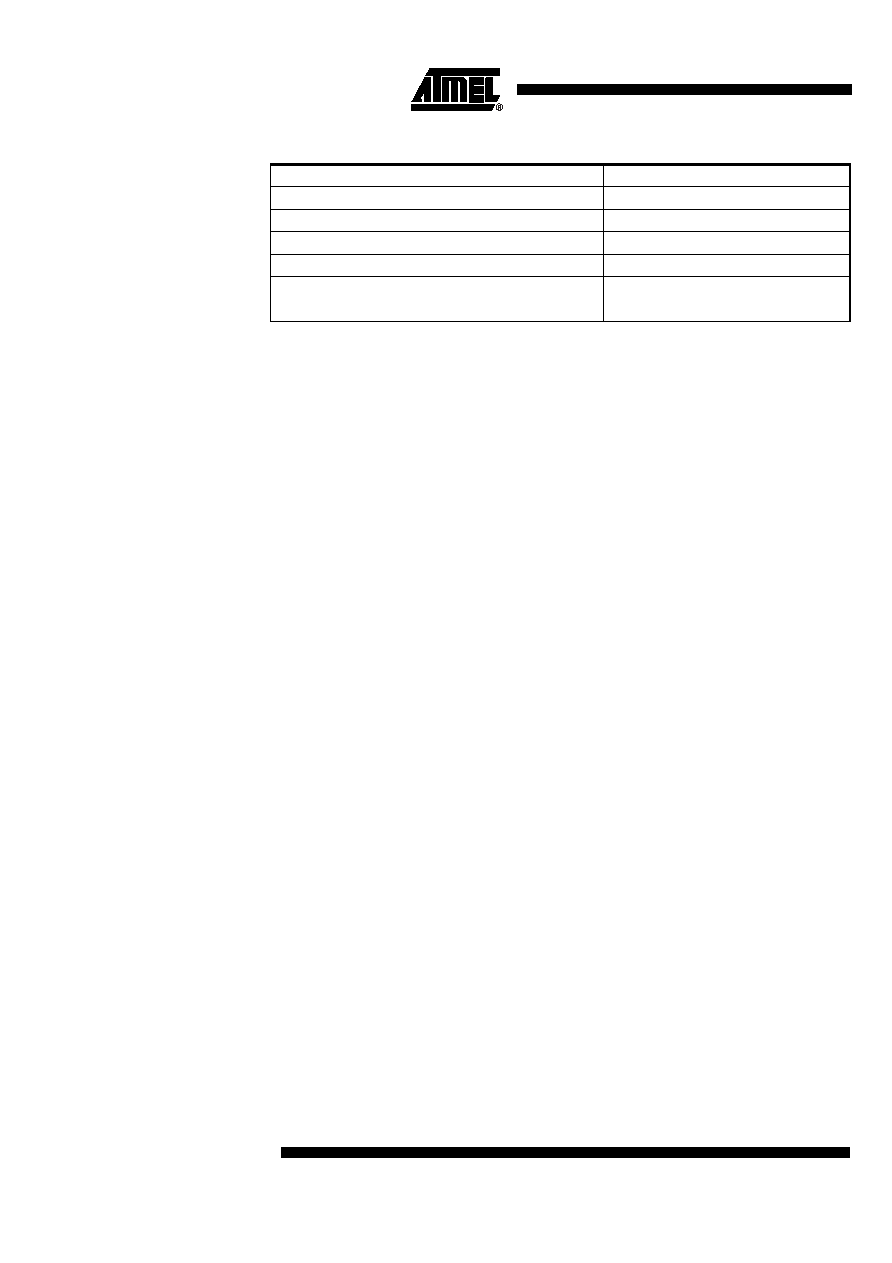
Table 1. AT40KEL040
Device
AT40KEL040
Usable Gates
40K - 50K
Rows x Columns
48 x 48
Cells
2,304
Registers
3,048(1)
RAM Bits
2304
I/O (max)
384
相關(guān)PDF資料 |
PDF描述 |
|---|---|
| 9305DMQB | 93 SERIES, ASYN POSITIVE EDGE TRIGGERED 4-BIT BINARY COUNTER, CDIP14 |
| 9308DMQB | 93 SERIES, DUAL LOW LEVEL TRIGGERED D LATCH, TRUE OUTPUT, CDIP24 |
| 9308FMQB | 93 SERIES, DUAL LOW LEVEL TRIGGERED D LATCH, TRUE OUTPUT, CDFP24 |
| 9309-00 | PRESCALER, UUC |
| 9309-01 | PRESCALER, CDSO8 |
相關(guān)代理商/技術(shù)參數(shù) |
參數(shù)描述 |
|---|---|
| 9304-01 | 制造商:PEREGRINE 制造商全稱:PEREGRINE 功能描述:1- 7 GHz Low Power CMOS Divide-by-2 Prescaler |
| 93-0404-R | 制造商:International Rectifier 功能描述:1063-2276-001 - Bulk |
| 930404X | 功能描述:LAMP HOLDER 制造商:visual communications company - vcc 系列:* 零件狀態(tài):有效 標(biāo)準(zhǔn)包裝:250 |
| 930404X710RN | 制造商:Lighting Components & Design Inc 功能描述:Lampholder; Bayonet; 3 W; Brass (Housing); 6 in. Length, 22 AWG; Solder Lug |
| 930404X724AN | 功能描述:PMI ROUND .660" INC 250V TAB AMB 制造商:visual communications company - vcc 系列:* 零件狀態(tài):在售 標(biāo)準(zhǔn)包裝:100 |
發(fā)布緊急采購,3分鐘左右您將得到回復(fù)。