- 您現(xiàn)在的位置:買賣IC網(wǎng) > PDF目錄164353 > 8P001SRV1301C25 EEPROM PDF資料下載
參數(shù)資料
| 型號: | 8P001SRV1301C25 |
| 元件分類: | EEPROM |
| 英文描述: | EEPROM |
| 中文描述: | EEPROM的 |
| 文件頁數(shù): | 8/10頁 |
| 文件大小: | 121K |
| 代理商: | 8P001SRV1301C25 |
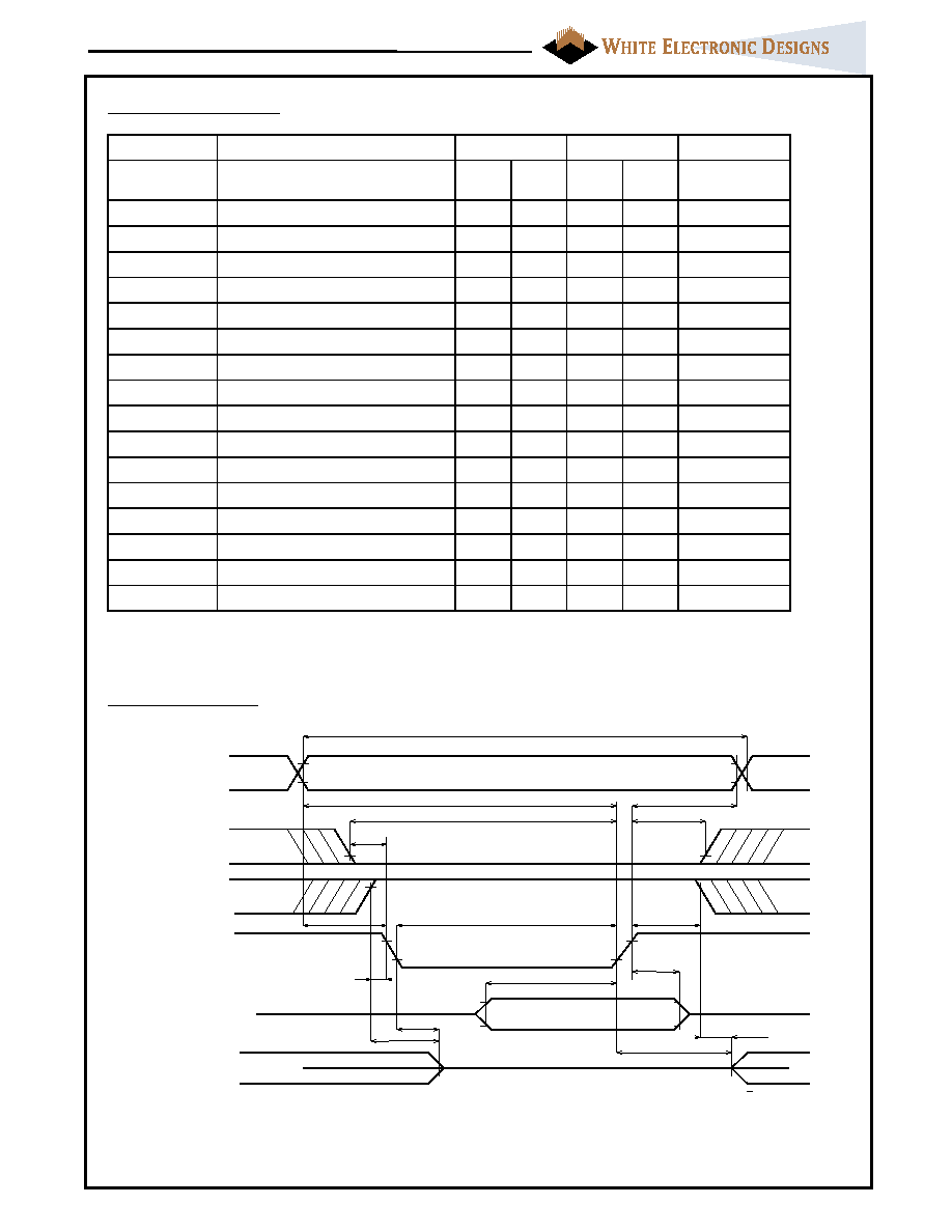
June 2000 Rev. 1 - ECO #12896
7
PCMCIA Flash Memory Card
SRV Series
PC Card Products
5.0V
3.3V
SYM
(PCMCIA)
Parameter
Min
Max
Min
Max
Unit
tCW
Write Cycle Time
150
250
ns
tw(WE)
Write Pulse Width
80
150
ns
tsu(A)
Address Setup Time
20
30
ns
tsu(A-WEH)
Address Setup Time for WE#
100
180
ns
tsu(CE-WEH)
Card Enable Setup Time for WE#
100
180
ns
tsu(D-WEH)
Data Setup Time for WE#
50
80
ns
th(D)
Data Hold Time
20
30
ns
trec(WE)
Write Recover Time
20
30
ns
tdis(WE)
Output Disable Time from WE#
75
100
ns
tdis(OE)
Output Disable Time from OE#
75
100
ns
ten(WE)
Output Enable Time from WE#
5
ns
tdis(OE)
Output Enable Time from OE#
5
ns
tsu(OE-WE)
Output Enable Setup from WE#
10
ns
th(OE-WE)
Output Enable Hold from WE#
10
ns
tsu(CE)
Card Enable Setup Time from OE#
0
ns
th(CE)
Card Enable Hold Time
20
ns
Note: AC timing diagrams and characteristics are guaranteed to meet or exceed PCMCIA 2.1 specifications.
Write Timing Diagram
Write Timing Parameters
th ( O E - W E )
NO T E 1
/C E 1 , /C E 2
NO T E 1
ts u ( C E - W E H )
tc ( W )
A [2 5 ::0 ], /R E G
tw ( W E )
td is ( W E )
th ( D )
D [ 15 : :0] ( D in )
DA T A I N P U T
ts u ( A )
ts u ( A - W E H )
/O E
ts u ( C E )
ts u ( D - W E H )
tr e c ( W E )
th ( C E )
ts u ( O E - W E )
td is ( O E )
D [ 15::0 ] ( D out )
te n ( O E )
te n ( W E )
NO T E 2
/W E
Notes:
1. Signal may be high or low in this area.
2. When the data I/O pins are in the output state, no signals shall be applied to the data pins (D15 - D0) by the host
system.
相關PDF資料 |
PDF描述 |
|---|---|
| 8P001SRV1301I15 | EEPROM |
| 8P001SRV1301I25 | EEPROM |
| 8P001SRV1302C15 | EEPROM |
| 8P001SRV1302C25 | EEPROM |
| 8P002SRV0101I25 | EEPROM |
相關代理商/技術(shù)參數(shù) |
參數(shù)描述 |
|---|---|
| 8P-03AFFM-QL5A01 | 功能描述:M8 CONN 制造商:amphenol ltw 系列:* 零件狀態(tài):在售 標準包裝:10 |
| 8P-03AFFM-QL5A02 | 功能描述:M8 CONN 制造商:amphenol ltw 系列:* 零件狀態(tài):在售 標準包裝:10 |
| 8P-03AFFM-QL5A05 | 功能描述:M8 CONN 制造商:amphenol ltw 系列:* 零件狀態(tài):在售 標準包裝:10 |
| 8P-03AFFM-QL5A10 | 功能描述:M8 CONN 制造商:amphenol ltw 系列:* 零件狀態(tài):在售 標準包裝:10 |
| 8P-03AFFM-QL5B01 | 功能描述:M8 CONN 制造商:amphenol ltw 系列:* 零件狀態(tài):在售 標準包裝:10 |
發(fā)布緊急采購,3分鐘左右您將得到回復。