- 您現(xiàn)在的位置:買賣IC網(wǎng) > PDF目錄162994 > 83511-02 (PEREGRINE SEMICONDUCTOR CORP) DC - 1500MHz Low Power CMOS Divide-by-2 Prescaler PDF資料下載
參數(shù)資料
| 型號: | 83511-02 |
| 廠商: | PEREGRINE SEMICONDUCTOR CORP |
| 元件分類: | 諧振器 |
| 英文描述: | DC - 1500MHz Low Power CMOS Divide-by-2 Prescaler |
| 中文描述: | PRESCALER, PDSO8 |
| 封裝: | PLASTIC, MSOP-8 |
| 文件頁數(shù): | 2/7頁 |
| 文件大小: | 264K |
| 代理商: | 83511-02 |
Product Specification
PE83511
Page 2 of 7
2003-2006 Peregrine Semiconductor Corp. All rights reserved.
Document No. 70-0113-03
│ UltraCMOS RFIC Solutions
Table 3. Absolute Maximum Ratings
Electrostatic Discharge (ESD) Precautions
When handling this UltraCMOS device, observe
the same precautions that you would use with
other ESD-sensitive devices. Although this device
contains circuitry to protect it from damage due to
ESD, precautions should be taken to avoid
exceeding the rating specified in Table 3.
Latch-Up Avoidance
Unlike conventional CMOS devices, UltraCMOS
devices are immune to latch-up.
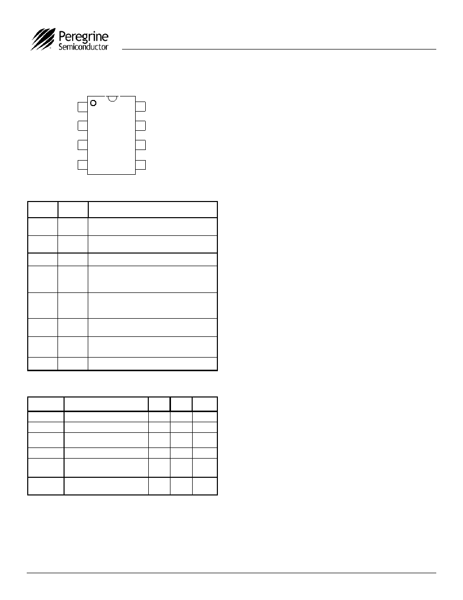
Figure 3. Pin Configuration (Top View)
Device Functional Considerations
The PE83511 divides an input signal, up to a
frequency of 1500 MHz, by a factor of two thereby
producing an output frequency at half the input
frequency. To work properly at higher frequency,
the input and output signals (pins 2, 7 & optional
5) must be AC coupled via an external capacitor.
The input may be DC coupled for low frequency
operation with care taken to remain within the
specified DC input range for the device.
The ground pattern on the board should be made
as wide as possible to minimize ground
impedance. See Figure 8 for a layout example.
OUTB Control
Pin 6 controls whether OUTB is enabled or
disabled. Pin 6 has an internal pull-up resistor.
With no connection (floating), OUTB is disabled.
By grounding pin 6, OUTB is enabled. By
enabling OUTB, this part will consume roughly
5 mA more current.
Absolute Maximum Ratings are those values
listed in the above table. Exceeding these values
may cause permanent device damage. Exposure
to absolute maximum ratings for extended periods
may affect device reliability.
Table 2. Pin Descriptions
8
PE83511
1
2
3
4
7
6
5
IN
GND
N/C
GND
OUT
VDD
CTL
OUT
8
Pin
No.
Pin
Name
Description
1
VDD
Power supply pin. Bypassing is required
(eg 1000 pF & 100 pF).
2
IN
Input signal pin. Should be coupled with a
capacitor (eg 1000 pF).
3
N/C
No connection. This pin should be left open.
4
GND
Ground pin. Ground pattern on the board
should be as wide as possible to reduce
ground impedance.
5
OUTB
Inverted divided frequency output. This pin
should be coupled with a capacitor
(eg 1000 pF).
6
CTL
Control pin. When grounded OUTB is
enabled.
7
OUT
Divided frequency output. This pin should
be coupled with a capacitor (eg 1000 pF).
8
GND
Ground Pin.
Symbol
Parameter/Conditions
Min
Max
Units
VDD
Supply voltage
4.0
V
Pin
Input Power
15
dBm
VIN
Voltage on input
-0.3
VDD
+0.3
V
TST
Storage temperature range
-65
150
°C
TOP
Operating temperature
range
-55
125
°C
VESD
ESD voltage (Human Body
Model, MIL-STD 883)
2000
V
相關(guān)PDF資料 |
PDF描述 |
|---|---|
| 83512-01 | DC - 1500 MHz Low Power CMOS Divide-by-4 Prescaler |
| 83512-02 | DC - 1500 MHz Low Power CMOS Divide-by-4 Prescaler |
| 83513-01 | DC - 1500 MHz Low Power CMOS Divide-by-8 Prescaler |
| 83513-02 | DC - 1500 MHz Low Power CMOS Divide-by-8 Prescaler |
| 83557-002 | INTERCONNECTION DEVICE |
相關(guān)代理商/技術(shù)參數(shù) |
參數(shù)描述 |
|---|---|
| 8351106 | 制造商: 功能描述: 制造商:undefined 功能描述: |
| 8-35111-1 | 功能描述:端子 NYL-RING 12-10 YEL #5/16 M8+ RoHS:否 制造商:AVX 產(chǎn)品:Junction Box - Wire to Wire 系列:9826 線規(guī):26-18 接線柱/接頭大小: 絕緣: 顏色:Red 型式:Female 觸點(diǎn)電鍍:Tin over Nickel 觸點(diǎn)材料:Beryllium Copper, Phosphor Bronze 端接類型:Crimp |
| 8-35111-5 | 制造商:TE Connectivity 功能描述:RING TONGUE TERM 10-12AWG 33.57MM 13.48MM TIN - Bulk |
| 8-35112-1 | 功能描述:端子 TRM PIDG R 12-10 3/8 TRM PIDG R 12-10 3/8 RoHS:否 制造商:AVX 產(chǎn)品:Junction Box - Wire to Wire 系列:9826 線規(guī):26-18 接線柱/接頭大小: 絕緣: 顏色:Red 型式:Female 觸點(diǎn)電鍍:Tin over Nickel 觸點(diǎn)材料:Beryllium Copper, Phosphor Bronze 端接類型:Crimp |
| 8351130 | 制造商: 功能描述: 制造商:undefined 功能描述: |
發(fā)布緊急采購,3分鐘左右您將得到回復(fù)。