- 您現(xiàn)在的位置:買賣IC網(wǎng) > PDF目錄162994 > 83501-12 (PEREGRINE SEMICONDUCTOR CORP) 3.5 GHz Low Power CMOS Divide-by-2 Prescaler PDF資料下載
參數(shù)資料
| 型號: | 83501-12 |
| 廠商: | PEREGRINE SEMICONDUCTOR CORP |
| 元件分類: | 諧振器 |
| 英文描述: | 3.5 GHz Low Power CMOS Divide-by-2 Prescaler |
| 中文描述: | PRESCALER, PDSO8 |
| 封裝: | MSOP-8 |
| 文件頁數(shù): | 2/8頁 |
| 文件大?。?/td> | 199K |
| 代理商: | 83501-12 |
Product Specification
PE83501
Page 2 of 8
2003-2006 Peregrine Semiconductor Corp. All rights reserved.
Document No. 70-0124-02
│ UltraCMOS RFIC Solutions
Table 2. Pin Descriptions
Table 3. Absolute Maximum Ratings
Electrostatic Discharge (ESD) Precautions
When handling this UltraCMOS device, observe
the same precautions that you would use with
other ESD-sensitive devices. Although this device
contains circuitry to protect it from damage due to
ESD, precautions should be taken to avoid
exceeding the rating specified in Table 3.
Latch-Up Avoidance
Unlike conventional CMOS devices, UltraCMOS
devices are immune to latch-up.
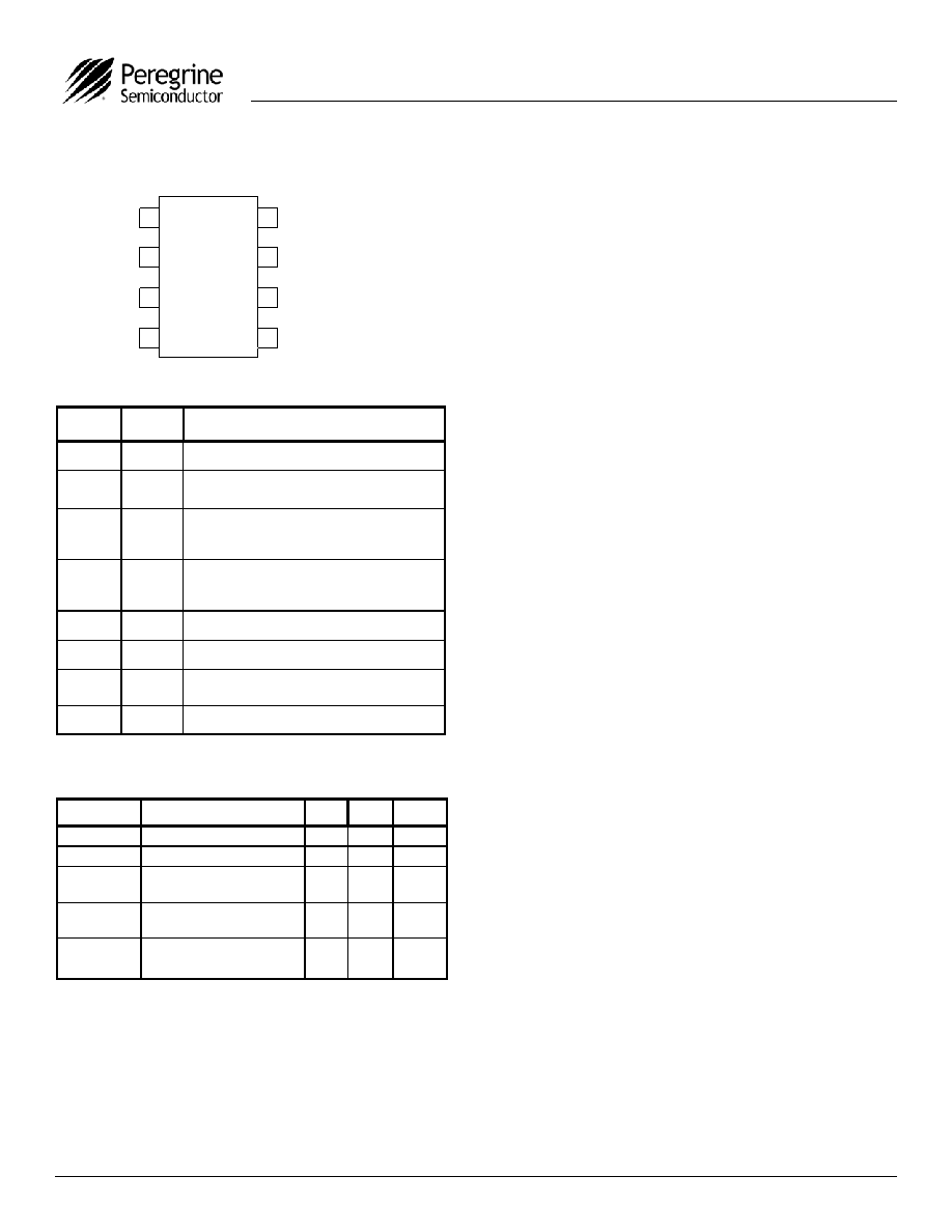
Figure 3. Pin Configuration (Top View)
Device Functional Considerations
The PE83501 divides a 400 MHz to 3.5 GHz input
signal by two, producing a 200 MHz to 1.75 GHz
output signal. To work properly, pin 3 must be
supplied with a bypass capacitor to ground. In
addition, the input and output signals (pins 2 & 7)
must be AC coupled via an external capacitor, as
shown in the test circuit in Figure 4.
The ground pattern on the board should be made
as wide as possible to minimize ground
impedance. See Figure 9 for a layout example.
Absolute Maximum Ratings are those values
listed in the above table. Exceeding these values
may cause permanent device damage. Exposure
to absolute maximum ratings for extended periods
may affect device reliability.
PE83501
1
2
3
4
8
7
6
5
Fin
GND
DEC
GND
Fout
VDD
GND
Pin
No.
Pin
Name
Description
1
VDD
Power supply pin. Bypassing is required.
2
Fin
Input signal pin. DC blocking capacitor
required (15 pF typical)
3
DEC
Power supply decoupling pin. Place a
capacitor as close as possible and connect
directly to the ground plane.
4
GND
Ground pin. Ground pattern on the board
should be as wide as possible to reduce
ground impedance.
5
GND
Ground pin.
6
GND
Ground pin.
7
Fout
Divided frequency output pin. DC blocking
capacitor required (47 pF typical)
8
GND
Ground pin.
Symbol
Parameter/Conditions
Min
Max
Units
VDD
Supply voltage
4.0
V
Pin
Input Power
15
dBm
TST
Storage temperature
range
-65
150
°C
TOP
Operating temperature
range
-55
125
°C
VESD
ESD voltage (Human
Body Model)
250
V
相關(guān)PDF資料 |
PDF描述 |
|---|---|
| 83502-21 | 3.5 GHz Low Power CMOS Divide-by-4 Prescaler |
| 83502-22 | 3.5 GHz Low Power CMOS Divide-by-4 Prescaler |
| 83503-21 | 3.5 GHz Low Power CMOS Divide-by-8 Prescaler |
| 83503-22 | 3.5 GHz Low Power CMOS Divide-by-8 Prescaler |
| 83511-01 | DC - 1500MHz Low Power CMOS Divide-by-2 Prescaler |
相關(guān)代理商/技術(shù)參數(shù) |
參數(shù)描述 |
|---|---|
| 8350-121603-16A | 制造商:Carling Technologies 功能描述:- Bulk |
| 8350-122004-60A | 制造商:Carling Technologies 功能描述:- Bulk |
| 83502 | 制造商:ERNI Electronics 功能描述:CODEZT 2 1 SELLBAG 100 |
| 83502-00 | 制造商:PEREGRINE 制造商全稱:PEREGRINE 功能描述:3.5 GHz Low Power UltraCMOS Divide-by-4 Prescaler Military Operating Temperature Range |
| 83502005 | 功能描述:基本/快動開關(guān) MAN PSH BTN 1PDT W3 83101 RoHS:否 制造商:Omron Electronics 觸點形式:SPDT 執(zhí)行器:Lever 電流額定值:5 A 電壓額定值 AC:250 V 電壓額定值 DC:30 V 功率額定值: 工作力:120 g IP 等級:IP 67 NEMA 額定值: 端接類型:Wire 安裝:Panel |
發(fā)布緊急采購,3分鐘左右您將得到回復(fù)。