- 您現(xiàn)在的位置:買賣IC網(wǎng) > PDF目錄378210 > 80960JD-33 (Intel Corp.) EMBEDDED 32-BIT MICROPROCESSOR PDF資料下載
參數(shù)資料
| 型號: | 80960JD-33 |
| 廠商: | Intel Corp. |
| 英文描述: | EMBEDDED 32-BIT MICROPROCESSOR |
| 中文描述: | 嵌入式32位微處理器 |
| 文件頁數(shù): | 16/78頁 |
| 文件大小: | 835K |
| 代理商: | 80960JD-33 |
第1頁第2頁第3頁第4頁第5頁第6頁第7頁第8頁第9頁第10頁第11頁第12頁第13頁第14頁第15頁當(dāng)前第16頁第17頁第18頁第19頁第20頁第21頁第22頁第23頁第24頁第25頁第26頁第27頁第28頁第29頁第30頁第31頁第32頁第33頁第34頁第35頁第36頁第37頁第38頁第39頁第40頁第41頁第42頁第43頁第44頁第45頁第46頁第47頁第48頁第49頁第50頁第51頁第52頁第53頁第54頁第55頁第56頁第57頁第58頁第59頁第60頁第61頁第62頁第63頁第64頁第65頁第66頁第67頁第68頁第69頁第70頁第71頁第72頁第73頁第74頁第75頁第76頁第77頁第78頁
80960JA/JF/JD/JT 3.3 V Microprocessor
16
Advance Information Datasheet
3.1
Pin Descriptions
This section describes the pins for the 80960Jx in the 132-pin ceramic Pin Grid Array (PGA)
package, 132-lead Plastic Quad Flatpack Package (PQFP) and 196-ball Mini Plastic Ball Grid
Array (MPBGA).
Section 3.1.1, “Functional Pin Definitions”, describes pin function; Section 3.1.2, “80960Jx
132-Lead PGA Pinout”, Section 3.1.3, “80960Jx 132-Lead PQFP Pinout” and Section 3.1.4,
“80960Jx 196-Ball MPBGA Pinout”, define the signal and pin locations for the supported package
types.
3.1.1
Functional Pin Definitions
Table 2 presents the legend for interpreting the pin descriptions which follow. Pins associated with
the bus interface are described in Table 3. Pins associated with basic control and test functions are
described in Table 4. Pins associated with the Interrupt Unit are described in Table 5.
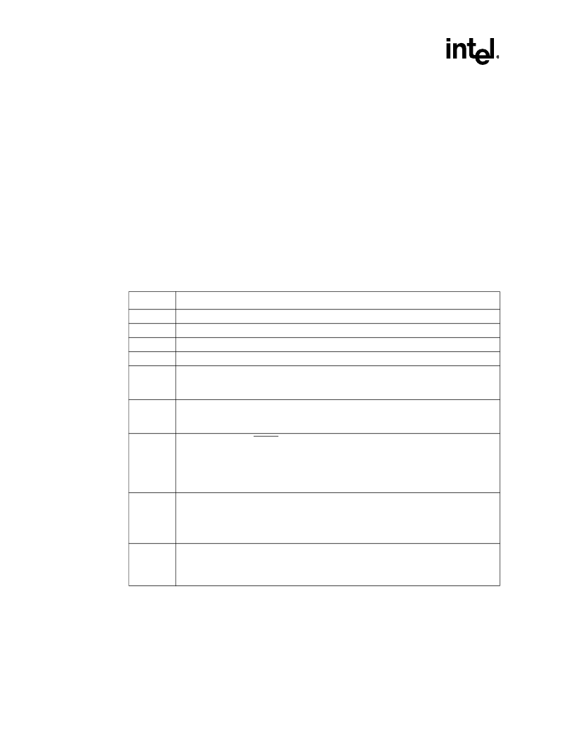
Table 2.
Pin Description Nomenclature
Symbol
Description
I
Input pin only.
O
Output pin only.
I/O
Pin can be either an input or output.
–
Pin must be connected as described.
S
Synchronous. Inputs must meet setup and hold times relative to CLKIN for proper operation.
S(E) Edge sensitive input
S(L) Level sensitive input
A (...)
Asynchronous. Inputs may be asynchronous relative to CLKIN.
A(E) Edge sensitive input
A(L) Level sensitive input
R (...)
While the processor’s RESET pin is asserted, the pin:
R(1) is driven to V
CC
R(0) is driven to V
R(Q) is a valid output
R(X) is driven to unknown state
R(H) is pulled up to V
CC
H (...)
While the processor is in the hold state, the pin:
H(1) is driven to V
CC
H(0) is driven to V
H(Q) Maintains previous state or continues to be a valid output
H(Z) Floats
P (...)
While the processor is halted, the pin:
P(1) is driven to V
CC
P(0) is driven to V
P(Q) Maintains previous state or continues to be a valid output
相關(guān)PDF資料 |
PDF描述 |
|---|---|
| 80960JD-40 | EMBEDDED 32-BIT MICROPROCESSOR |
| 80960JD-50 | EMBEDDED 32-BIT MICROPROCESSOR |
| 80960JF-16 | EMBEDDED 32-BIT MICROPROCESSOR |
| 80960JF-25 | EMBEDDED 32-BIT MICROPROCESSOR |
| 80960JF-33 | EMBEDDED 32-BIT MICROPROCESSOR |
相關(guān)代理商/技術(shù)參數(shù) |
參數(shù)描述 |
|---|---|
| 80960JD-40 | 制造商:INTEL 制造商全稱:Intel Corporation 功能描述:EMBEDDED 32-BIT MICROPROCESSOR |
| 80960JD-50 | 制造商:INTEL 制造商全稱:Intel Corporation 功能描述:EMBEDDED 32-BIT MICROPROCESSOR |
| 80960JF | 制造商:INTEL 制造商全稱:Intel Corporation 功能描述:3.3 V EMBEDDED 32-BIT MICROPROCESSOR |
| 80960JF-16 | 制造商:INTEL 制造商全稱:Intel Corporation 功能描述:EMBEDDED 32-BIT MICROPROCESSOR |
| 80960JF-25 | 制造商:INTEL 制造商全稱:Intel Corporation 功能描述:EMBEDDED 32-BIT MICROPROCESSOR |
發(fā)布緊急采購,3分鐘左右您將得到回復(fù)。