- 您現(xiàn)在的位置:買賣IC網(wǎng) > PDF目錄378210 > 80930AD (Intel Corp.) Universal Serial Bus Microcontroller(通用串行總線微控制器) PDF資料下載
參數(shù)資料
| 型號: | 80930AD |
| 廠商: | Intel Corp. |
| 英文描述: | Universal Serial Bus Microcontroller(通用串行總線微控制器) |
| 中文描述: | 通用串行總線控制器(通用串行總線微控制器) |
| 文件頁數(shù): | 18/38頁 |
| 文件大小: | 226K |
| 代理商: | 80930AD |
第1頁第2頁第3頁第4頁第5頁第6頁第7頁第8頁第9頁第10頁第11頁第12頁第13頁第14頁第15頁第16頁第17頁當前第18頁第19頁第20頁第21頁第22頁第23頁第24頁第25頁第26頁第27頁第28頁第29頁第30頁第31頁第32頁第33頁第34頁第35頁第36頁第37頁第38頁
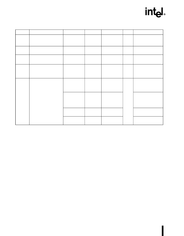
14
ADVANCE INFORMATION
8x930Ax UNIVERSAL SERIAL BUS (USB) MICROCONTROLLER
I
TL
Logical 1-to-0
Transition Current
(Port 1, 2,3)
-650
μA
V
IN
= 2.0 V
R
RST
RST Pulldown
Resistor
40
225
K
C
IO
10
pF
F
OSC
= 12 MHz
T
A
= 25°C
I
PD
Powerdown Current
— Normal powerdown
— USB suspend
25
145
50
175
μA
I
DL
(5)
Idle Mode I
CC
40
mA
PLLSEL = 110
3MHz – FS
(in low clock mode)
100
PLLSEL = 110
12MHz – FS
(not in low clock
mode)
30
PLLSEL = 001
3MHz – LS
55
PLLSEL = 100
6 MHz – LS
Table 9. DC Characteristics at Operating Conditions (Continued)
Symbol
Parameter
Min
Typical (1)
Max
Units
Test Conditions
NOTE:
1.
2.
Typical values are obtained using V
= 5.0V, T
A
= 25°C and are not guaranteed.
Under steady state (non-transient) conditions, I
OL
must be externally limited as follows:
Maximum I
OH
per port pin:10 mA
Maximum I
per 8-bit port:
Port 0: 26 mA
Ports 1-3: 15 mA
Maximum Total I
for all output pins: 71 mA
If I
exceeds the test conditions, V
may exceed the related specification. Pins are not guaranteed
to sink current greater than the listed test conditions.
Capacitive loading on Ports 0 and 2 may cause spurious noise pulses above 0.4 V on the low-level
outputs of ALE and Ports 1, 2 and 3. The noise is due to external bus capacitance discharging into the
Port 0 and Port 2 pins when these pins change from 1 to 0. In applications where capacitive loading
exceeds 100pF, the noise pulses on these signals may exceed 0.8 V. It may be desirable to qualify
ALE or other signals with a Schmitt Trigger or CMOS-level input logic.
Capacitive loading on Ports 0 and 2 cause the V
OH
on ALE and PSEN to drop below the V
CC
specifica-
tion when the address lines are stabilizing.
The abbreviations “LS” and “FS” indicate “Low Speed” and “Full Speed,” respectively.
3.
4.
5.
相關(guān)PDF資料 |
PDF描述 |
|---|---|
| 80931AA | Universal Serial Bus Peripheral Controller(通用串行總線HUB外設(shè)微控制器) |
| 80931HA | Universal Serial Bus Peripheral Controller(通用串行總線HUB外設(shè)微控制器) |
| 8095-90 | MCS-96 809X-90, 839X-90 |
| 8095BH | COMMERCIAL/EXPRESS HMOS MICROCONTROLLER |
| 8096BH | COMMERCIAL/EXPRESS HMOS MICROCONTROLLER |
相關(guān)代理商/技術(shù)參數(shù) |
參數(shù)描述 |
|---|---|
| 80931 | 制造商:JOHANSON 功能描述:* |
| 8093-1 | 制造商:JOHANS 功能描述: |
| 809319-1 | 制造商:TE Connectivity 功能描述:COVER, DRIVE ARM - Bulk |
| 80932 | 功能描述:SET TL MECH 1/4,3/8,1/2DR 165PC 制造商:apex tool group 系列:* 零件狀態(tài):在售 標準包裝:2 |
| 809320-1 | 功能描述:手工工具 PIN, DRIVE RoHS:否 制造商:Molex 產(chǎn)品:Extraction Tools 類型: 描述/功能:Extraction tool |
發(fā)布緊急采購,3分鐘左右您將得到回復(fù)。