- 您現(xiàn)在的位置:買賣IC網(wǎng) > PDF目錄294400 > 7P256FLG0300I20 VOLTAGE DETECTOR W/PUSH-PULL ACTIVE HIGH OUTPUT & Oms TIMEOUT, -40C to +125C, 5-SOT-23, T/R PDF資料下載
參數(shù)資料
| 型號(hào): | 7P256FLG0300I20 |
| 英文描述: | VOLTAGE DETECTOR W/PUSH-PULL ACTIVE HIGH OUTPUT & Oms TIMEOUT, -40C to +125C, 5-SOT-23, T/R |
| 中文描述: | 周邊雜項(xiàng) |
| 文件頁(yè)數(shù): | 8/13頁(yè) |
| 文件大小: | 125K |
| 代理商: | 7P256FLG0300I20 |
第1頁(yè)第2頁(yè)第3頁(yè)第4頁(yè)第5頁(yè)第6頁(yè)第7頁(yè)當(dāng)前第8頁(yè)第9頁(yè)第10頁(yè)第11頁(yè)第12頁(yè)第13頁(yè)

August 2000 Rev. 3 - ECO #13132
4
PCMCIA Flash Memory Card
FLG Series
PC Card Products
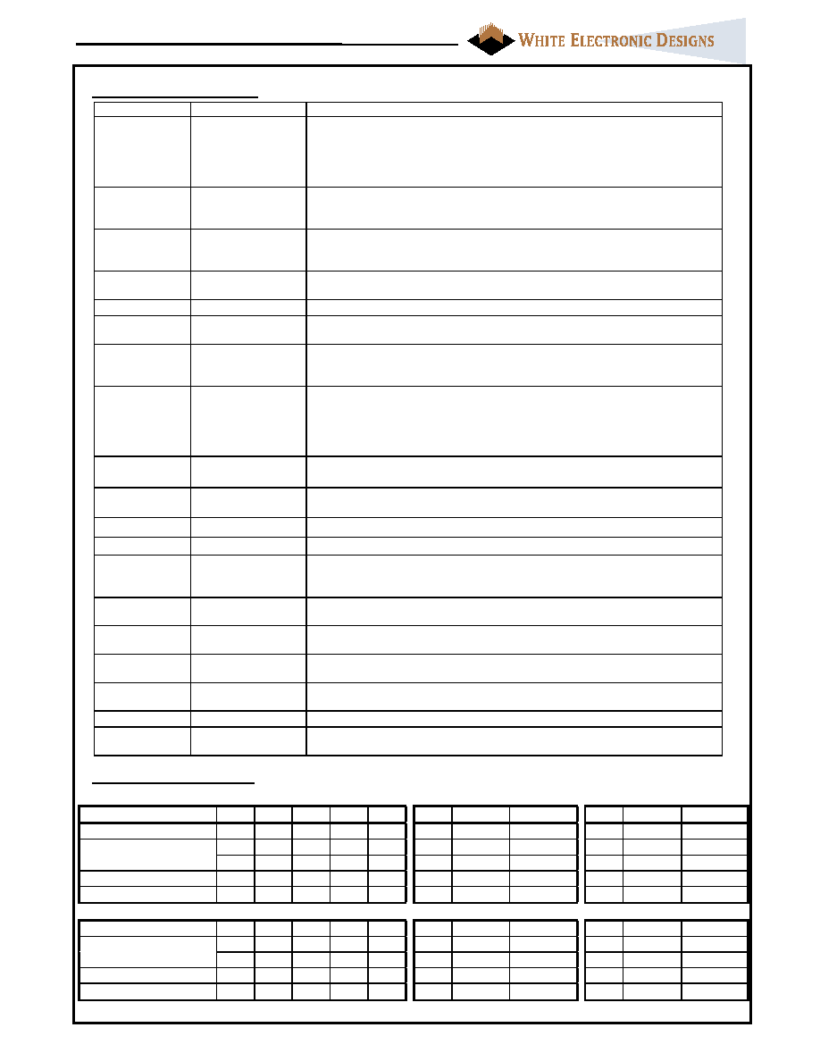
Symbol
Type
Name and Function
A0 - A25
INPUT
ADDRESS INPUTS: A0 through A25 enable direct addressing of up to
64MB of memory on the card. Signal A0 is not used in word access mode.
The memory will wrap at the card density boundary (see PINOUT, note 3).
The system should not try to access memory beyond the card density.
A25 is the most significant bit. A23 – A25 are not connected.
DQ0 - DQ15
INPUT/OUTPUT
DATA INPUT/OUTPUT: DQ0 THROUGH DQ15 constitute the bi-
directional databus. DQ0 – DQ7 constitute the lower (even) byte and DQ8
– DQ15 the upper (odd) byte. DQ15 is the MSB.
CE1#, CE2#
INPUT
CARD ENABLE 1 AND 2: CE1# enables even byte accesses, CE2#
enables odd byte accesses. Multiplexing A0, CE1# and CE2# allows 8-bit
hosts to access all data on DQ0 - DQ7.
OE#
INPUT
OUTPUT ENABLE: Active low signal gating read data from the memory
card.
WE#
INPUT
WRITE ENABLE: Active low signal gating write data to the memory card.
RDY/BSY#
N.C.
READY/BUSY OUTPUT: Indicates status of internally timed erase or
program algorithms. This signal is not connected.
CD1#, CD2#
OUTPUT
CARD DETECT 1 and 2: Provide card insertion detection. These signals
are internally connected to ground on the card. The host shall monitor
these signals to detect card insertion (pulled-up on host side).
WP
OUTPUT
WRITE PROTECT: Write protect reflects the status of the Write Protect
switch on the memory card. WP set to high = write protected, providing
internal hardware write lockout to the Flash array.
If card does not include optional write protect switch, this signal will be
pulled low internally indicating write protect = "off".
VPP1
PROGRAM/ERASE POWER SUPPLY: Provides programming voltages
12.0V for lower byte (D0 – D7) memory components.
VPP2
PROGRAM/ERASE POWER SUPPLY: Provides programming voltages
12.0V for upper byte (D8 – D15) memory components.
VCC
CARD POWER SUPPLY: (5.0V).
GND
CARD GROUND
REG#
INPUT
ATTRIBUTE MEMORY SELECT : Active low signal, enables access to
Attribute Memory Plane, occupied by Card Information Structure and Card
Registers.
RST
N.C.
RESET: Active high signal for placing cards in Power-on default state.
This signal is not connected.
WAIT#
OUTPUT
WAIT: This signal is pulled high internally for compatibility. No wait states
are generated.
BVD1, BVD2
OUTPUT
BATTERY VOLTAGE DETECT: These signals are pulled high to maintain
SRAM card compatibility.
VS1, VS2
OUTPUT
VOLTAGE SENSE: Notifies the host socket of the card's VCC
requirements. VS1 and VS2 are open to indicate a 5V card.
RFU
RESERVED FOR FUTURE USE
N.C.
NO INTERNAL CONNECTION TO CARD: pin may be driven or left
floating
Card Signal Description
READ function
Common Memory
Attribute Memory
Function Mode
/CE2
/CE1
A0
/OE
/WE
/REG
D15-D8
D7-D0
/REG
D15-D8
D7-D0
Standby Mode
HH
X
High-Z
X
High-Z
Byte Access (8 bits)
HL
L
H
High-Z
Even-Byte
L
High-Z
Even-Byte
HL
H
High-Z
Odd-Byte
L
High-Z
Not Valid
Word Access (16 bits)
LL
X
L
H
Odd-Byte Even-Byte
L
Not Valid
Even-Byte
Odd-Byte Only Access
LH
X
L
H
Odd-Byte
High-Z
L
Not Valid
High-Z
WRITE function
*
Standby Mode
HH
X
XX
X
XX
Byte Access (8 bits)
HL
L
H
L
H
XEven-Byte
L
X
Even-Byte
HL
H
L
H
XOdd-Byte
L
XX
Word Access (16 bits)
LL
X
H
L
H
Odd-Byte Even-Byte
L
X
Even-Byte
Odd-Byte Only Access
LH
X
H
L
H
Odd-Byte
X
L
XX
Functional Truth Table
* Require proper programming voltages (Vpp1, Vpp2). Program or Erase with an invalid Vpp should not be attempted.
相關(guān)PDF資料 |
PDF描述 |
|---|---|
| 7P256FLG0301C15 | Micro Power Voltage detector, w/push pull active high, -40C to +125C, 5-SOT-23, T/R |
| 7P256FLG0301C20 | Peripheral Miscellaneous |
| 7P256FLG0301I15 | VOLTAGE DETECTOR W/PUSH-PULL ACTIVE HIGH OUTPUT & 2ms TIMEOUT, -40C to +125C, 5-SOT-23, T/R |
| 7P256FLG0301I20 | VOLTAGE DETECTOR W/PUSH-PULL ACTIVE HIGH OUTPUT & Oms TIMEOUT, -40C to +125C, 5-SOT-23, T/R |
| 7P256FLG0302C15 | MICRO POWER VOLTAGE DETECTOR, W/PUSH PULL ACTIVE HIGH, -40C to +125C, 4-SOT-143, T/R |
相關(guān)代理商/技術(shù)參數(shù) |
參數(shù)描述 |
|---|---|
| 7P256FLG0301C15 | 制造商:未知廠家 制造商全稱:未知廠家 功能描述:Peripheral Miscellaneous |
| 7P256FLG0301C20 | 制造商:未知廠家 制造商全稱:未知廠家 功能描述:Peripheral Miscellaneous |
| 7P256FLG0301I15 | 制造商:未知廠家 制造商全稱:未知廠家 功能描述:Peripheral Miscellaneous |
| 7P256FLG0301I20 | 制造商:未知廠家 制造商全稱:未知廠家 功能描述:Peripheral Miscellaneous |
| 7P256FLG0302C15 | 制造商:未知廠家 制造商全稱:未知廠家 功能描述:Peripheral Miscellaneous |
發(fā)布緊急采購(gòu),3分鐘左右您將得到回復(fù)。