- 您現(xiàn)在的位置:買賣IC網(wǎng) > PDF目錄294396 > 7P0080601C15 EEPROM PDF資料下載
參數(shù)資料
| 型號: | 7P0080601C15 |
| 元件分類: | EEPROM |
| 英文描述: | EEPROM |
| 中文描述: | EEPROM的 |
| 文件頁數(shù): | 6/11頁 |
| 文件大?。?/td> | 111K |
| 代理商: | 7P0080601C15 |
August 2000 Rev. 3 - ECO #13135
4
PCMCIA Flash Memory Card
FVB Series
PC Card Products
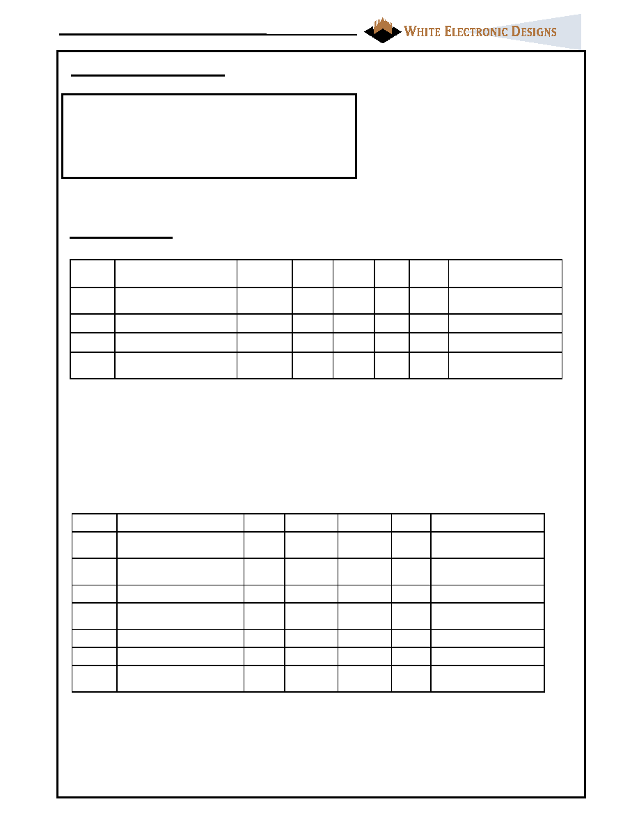
Absolute Maximum Ratings (1)
Operating Temperature TA (ambient)
Commercial
0°C to +60 °C
Industrial
-40°C to +85 °C
Storage Temperature
-40°C to +85 °C
Voltage on any pin relative to VSS
-0.5V to VCC+0.5V
VCC supply Voltage relative to VSS
-0.5V to +7.0V
Note:
(1) Stress greater than those listed under “Absolute
Maximum ratings” may cause permanent damage to
the device. This is a stress rating only and functional
operation at these or any other conditions greater
than those indicated in the operational sections of
this specification is not implied. Exposure to absolute
maximum rating conditions for extended periods
may affect reliability.
Symbol Parameter
Density
(Mbytes)
Notes
Typ
(3)
Max
Units
Test Conditions
ICCR
VCC Read Current
4,8,16
40
mA
VCC = 5.25V
tcycle = 150ns
ICCW
VCC Program Current
4,8,16
65
mA
ICCE
VCC Erase Current
4,8,16
65
mA
ICCS
VCC Standby Current
For max capacity 16MB
4,8,16
2
10
100
A
VCC = 5.25V
Control Signals = VCC
Notes:
1. All currents are for Byte mode and are RMS values unless otherwise specified.
2. Control Signals: CE
1#, CE2#, OE#, WE#, REG#.
3. Typical: VCC = 5V, T = +25C.
CMOS Test Conditions: VIL = VSS ± 0.2V, VIH = VCC ± 0.2V
DC Characteristics (1)
Symbol
Parameter
Notes
Min
Max
Units
Test Conditions
ILI
Input Leakage Current
1,2
±20
A
VCC = VCCMAX
Vin =VCC or VSS
ILO
Output Leakage Current
1
±20
A
VCC = VCCMAX
Vout =VCC or VSS
VIL
Input Low Voltage
1
0
0.8
V
VIH
Input High Voltage
1
3.85
VCC+0.
5
V
VOL
Output Low Voltage
1
0.4
V
IOL = 3.2mA
VOH
Output High Voltage
1
VCC-0.4
VCC
V
IOH = -2.0mA
VLKO
VCC Erase/Program
Lock Voltage
13.2
4.2
V
Notes:
1. Values are the same for byte and word wide modes for all card densities.
2. Exceptions: Leakage currents on CE1#, CE2#, OE#, REG# and WE# will be < 500 A when VIN = GND
due to internal pull-up resistors. Leakage currents on RST will be <150A when VIN=VCC due to
internal pull-down resistor.
相關PDF資料 |
PDF描述 |
|---|---|
| 7P0080601I15 | EEPROM |
| 7P0160500C15 | EEPROM |
| 7P0160500I15 | EEPROM |
| 7P0160501C15 | EEPROM |
| 7P0160501I15 | EEPROM |
相關代理商/技術參數(shù) |
參數(shù)描述 |
|---|---|
| 7P-10.000MBP-T | 功能描述:OSC TCXO 10.000MHZ CMOS SMD 制造商:txc corporation 系列:* 零件狀態(tài):在售 標準包裝:1,000 |
| 7P102V330A052 | 制造商:CDE 制造商全稱:Cornell Dubilier Electronics 功能描述:Type 7P 55 ∑C Photoflash, High-Energy, Long Life, Aluminum |
| 7P102V330N042 | 制造商:CDE 制造商全稱:Cornell Dubilier Electronics 功能描述:Type 7P 55 ∑C Photoflash, High-Energy, Long Life, Aluminum |
| 7P102V360A052 | 功能描述:鋁質電解電容器-管理單元 1000uF 360V PHOTO RoHS:否 制造商:Nichicon 電容:470 uF 容差:20 % 電壓額定值:450 V ESR: 工作溫度范圍:- 25 C to + 105 C 系列:AR 直徑:35 mm 長度:45 mm 引線間隔:10 mm 產(chǎn)品:General Purpose Electrolytic Capacitors |
| 7P122V330A052 | 制造商:CDE 制造商全稱:Cornell Dubilier Electronics 功能描述:Type 7P 55 ∑C Photoflash, High-Energy, Long Life, Aluminum |
發(fā)布緊急采購,3分鐘左右您將得到回復。