- 您現(xiàn)在的位置:買賣IC網(wǎng) > PDF目錄360547 > 7LVC841APWDH (NXP SEMICONDUCTORS) 10-bit transparent latch with 5-volt tolerant inputs/outputs 3-State PDF資料下載
參數(shù)資料
| 型號: | 7LVC841APWDH |
| 廠商: | NXP SEMICONDUCTORS |
| 元件分類: | 通用總線功能 |
| 英文描述: | 10-bit transparent latch with 5-volt tolerant inputs/outputs 3-State |
| 中文描述: | LVC/LCX/Z SERIES, 10-BIT DRIVER, TRUE OUTPUT, PDSO24 |
| 文件頁數(shù): | 2/10頁 |
| 文件大?。?/td> | 101K |
| 代理商: | 7LVC841APWDH |
Philips Semiconductors
Product specification
74LVC841A
10-bit transparent latch with 5-volt tolerant
inputs/outputs (3-State)
2
1998 Jun 17
853-2071 19589
FEATURES
5-volt tolerant inputs/outputs, for interfacing with 5-volt logic
Wide supply voltage range of 1.2 V to 3.6 V
In accordance with the JEDEC standard no. 8-1 A
Inputs accept voltages up to 5.5 V
CMOS low power consumption
Direct interface with TTL levels
Flow-through pin-out architecture
DESCRIPTION
The 74LVC841A is a low-power, low-voltage, Si-gate CMOS device
and superior to most advanced CMOS compatible TTL families.
Inputs can be driven from either 3.3 V or 5 V devices. In 3-State
operation, outputs can handle 5 V. This feature allows the use of
these devices as translators in a mixed 3.3 V/5 V environment. The
74LVC841A is a 10-bit transparent latch featuring separate D-type
inputs for each latch and 3-State outputs for bus oriented
applications. A latch enable (LE) input and an output enable (OE)
input are common to all internal latches. The 74LVC841A consists of
ten transparent latches with 3-State true outputs. When LE is HIGH,
data at the D
n
inputs enters the latches. In this condition the latches
are transparent, i.e., a latch output will change each time its
corresponding D-input changes. When LE is LOW the latches store
the information that was present at the D-inputs a set-up time
preceding the HIGH-to-LOW transition of LE. When OE is LOW, the
contents of the ten latches are available at the outputs.
When OE is HIGH, the outputs go to the high impedance OFF-state.
Operation of the OE input does not affect the state of the latches.
QUICK REFERENCE DATA
GND = 0 V; T
amb
= 25
°
C; t
r
=t
f
≤
2.5 ns
SYMBOL
PARAMETER
CONDITIONS
TYPICAL
UNIT
t
PHL
/t
PLH
Propagation delay
D
to Q
n
;
LE to Q
n
Input capacitance
C
L
= 50 pF;
V
CC
= 3.3 V
4.5
5.0
ns
C
I
C
PD
NOTE:
1
5.0
pF
Power dissipation capacitance per latch
V
I
= GND to V
CC1
22
pF
C
PD
is used to determine the dynamic power dissipation (P
D
in
μ
W)
P
D
= C
PD
×
V
CC2
×
f
i
(C
L
×
V
CC2
×
f
o
) where:
f
i
= input frequency in MHz; C
L
= output load capacity in pF;
f
o
= output frequency in MHz; V
CC
= supply voltage in V;
(C
L
×
V
CC2
×
f
o
) = sum of the outputs.
ORDERING INFORMATION
PACKAGES
TEMPERATURE RANGE
OUTSIDE NORTH AMERICA
NORTH AMERICA
PKG. DWG. #
24-Pin Plastic SO
–40
°
C to +125
°
C
74LVC841A D
74LVC841A D
SOT137-1
24-Pin Plastic SSOP Type II
–40
°
C to +125
°
C
74LVC841A DB
74LVC841A DB
SOT340-1
24-Pin Plastic TSSOP Type I
–40
°
C to +125
°
C
74LVC841A PW
7LVC841APW DH
SOT355-1
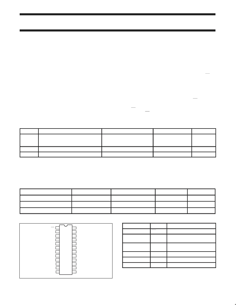
PIN CONFIGURATION
24
23
1
SV01723
D
0
D
1
D
2
D
3
D
4
D
5
D
6
D
7
D
8
D
9
GND
Q
0
Q
1
Q
2
Q
3
Q
4
Q
5
Q
6
Q
7
Q
8
Q
9
LE
V
CC
2
3
4
5
6
7
8
9
10
11
12
20
19
21
22
18
17
16
15
14
13
OE
PIN DESCRIPTION
PIN NUMBER
SYMBOL
NAME AND FUNCTION
1
OE
Output enable input (active Low)
2, 3, 4, 5, 6, 7, 8,
9, 10, 11
D
0
to D
9
Data inputs
23, 22, 21, 20, 19,
18, 17, 16, 15, 14
Q
0
to Q
9
3-state latch outputs
12
GND
Ground (0 V)
13
LE
Latch enable input (active HIGH)
24
V
CC
Positive supply voltage
相關(guān)PDF資料 |
PDF描述 |
|---|---|
| 7LVT2241PWDH | 3.3V Octal buffer/line driver with 30ohm series termination resistors; 3-State |
| 7LVT2244PWDH | 3.3V Octal buffer/line driver with 30ohm series termination resistors 3-State |
| 7LVT2245PWDH | 3.3V Octal transceiver with 30ohm termination resistors 3-State |
| 7LVT244APWDH | 3.3V Octal buffer/line driver 3-State |
| 7LVT244BPWDH | 3.3V Octal buffer/line driver 3-State |
相關(guān)代理商/技術(shù)參數(shù) |
參數(shù)描述 |
|---|---|
| 7LVT2241PWDH | 制造商:PHILIPS 制造商全稱:NXP Semiconductors 功能描述:3.3V Octal buffer/line driver with 30ohm series termination resistors; 3-State |
| 7LVT2244PWDH | 制造商:PHILIPS 制造商全稱:NXP Semiconductors 功能描述:3.3V Octal buffer/line driver with 30ohm series termination resistors 3-State |
| 7LVT2245PWDH | 制造商:PHILIPS 制造商全稱:NXP Semiconductors 功能描述:3.3V Octal transceiver with 30ohm termination resistors 3-State |
| 7LVT244APWDH | 制造商:PHILIPS 制造商全稱:NXP Semiconductors 功能描述:3.3V Octal buffer/line driver 3-State |
| 7LVT244BPWDH | 制造商:PHILIPS 制造商全稱:NXP Semiconductors 功能描述:3.3V Octal buffer/line driver 3-State |
發(fā)布緊急采購,3分鐘左右您將得到回復(fù)。