- 您現(xiàn)在的位置:買賣IC網(wǎng) > PDF目錄369357 > 7B991RPFE (MAXWELL TECHNOLOGIES) Programmable Skew Clock Buffer (PSCB) PDF資料下載
參數(shù)資料
| 型號(hào): | 7B991RPFE |
| 廠商: | MAXWELL TECHNOLOGIES |
| 元件分類: | 時(shí)鐘及定時(shí) |
| 英文描述: | Programmable Skew Clock Buffer (PSCB) |
| 中文描述: | PLL BASED CLOCK DRIVER, 8 TRUE OUTPUT(S), 0 INVERTED OUTPUT(S), DFP32 |
| 封裝: | RAD PAK, DFP-16 |
| 文件頁(yè)數(shù): | 8/17頁(yè) |
| 文件大?。?/td> | 253K |
| 代理商: | 7B991RPFE |
第1頁(yè)第2頁(yè)第3頁(yè)第4頁(yè)第5頁(yè)第6頁(yè)第7頁(yè)當(dāng)前第8頁(yè)第9頁(yè)第10頁(yè)第11頁(yè)第12頁(yè)第13頁(yè)第14頁(yè)第15頁(yè)第16頁(yè)第17頁(yè)

M
8
All data sheets are subject to change without notice
2002 Maxwell Technologies.
All rights reserved.
Programmable Skew Clock Buffer (PSCB)
7B991
09.23.02 Rev 4
B
LOCK
D
IAGRAM
D
ESCRIPTION
Phase Frequency Detector and Filter
These two blocks accept inputs fromthe reference frequency (REF) input and the feedback (FB) input and generate
correction information to control the frequency of the Voltage-Controlled Oscillator (VCO). These blocks, along with
the VCO, forma Phase-Locked Loop (PLL) that tracks the incomng REF signal.
VCO and Time Unit Generator
The VCO accepts analog control inputs fromthe PLL filter block and generates a frequency that is used by the time
unit generator to create discrete time units that are selected in the skew select matrix. The operational range of the
VCO is determned by the FS control pin. The time unit (t
U
) is determned by the operating frequency of the device and
the level of the FS pin as shown in Table 1.
Skew Select Matrix
The skew select matrix is comprised of four independent sections. Each section has two low-skew high-fanout driv-
ers(xQ0, xQ1), and two corresponding three-level function select (xF0, xF1) inputs. Table 9 below shows the nine pos-
sible output functions for each section as determned by the function select inputs. All times are measured with respect
to the REF input assumng that the output connected to the FB input has 0t
U
selected.
T
ABLE
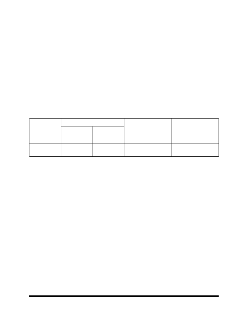
8. 7B991 F
REQUENCY
R
ANGE
S
ELECT
AND
t
U
C
ALCULATION1
fNOM(MH
Z
)
1. For all three state inputs. HIGH indicates a connection to V
CC
. LOW indicates a connection to GND, and MID indicates an
open connection. Internal termnation circuitry holds an unconnected input to V
CC
/2.
2. The level to be set of FS is determned by the
“
normal
”
operating frequency (f
NOM
) of the V
CO
and Time Unit Generator (see
Logic Block Diagram. Nomnal frequency (f
NOM
) always appears at 1Q0 and the other outputs when they are operated in their
undivided modes (See Table 9). The frequency appearing at the REF and FB inputs will be f
NOM
when the output connected to
FB is undivided. The frequency appearing at the REF and FB inputs will be f
NOM
/2 or f
NOM
/4 when the part is configured for a
frequency multiplication by using a divided output as the FB input.
3. When the FS pin is selected HIGH, the REF input must not transition upon power-up until V
CC
has reached 4.3V.
FS
2,3
t
U
= 1/fNOM
X
N
WHERE
N =
A
PPROXIMATE
F
REQUENCY
(MH
Z
)
AT
WHICH
t
U
= 1.0 ns
M
IN
M
AX
LOW
MID
HIGH
15
25
40
30
50
80
44
26
16
22.7
38.5
62.5
相關(guān)PDF資料 |
PDF描述 |
|---|---|
| 7B991RPFI | Programmable Skew Clock Buffer (PSCB) |
| 7B991RPFS | Programmable Skew Clock Buffer (PSCB) |
| 7B991 | Programmable Skew Clock Buffer (PSCB) |
| 7BT2F9A-361 | HIGH CAPACITY ENVIRONMENTALLY SEALED |
| 7BT2 | HIGH CAPACITY ENVIRONMENTALLY SEALED |
相關(guān)代理商/技術(shù)參數(shù) |
參數(shù)描述 |
|---|---|
| 7B991RPFI | 制造商:MAXWELL 制造商全稱:Maxwell Technologies 功能描述:Programmable Skew Clock Buffer (PSCB) |
| 7B991RPFS | 制造商:MAXWELL 制造商全稱:Maxwell Technologies 功能描述:Programmable Skew Clock Buffer (PSCB) |
| 7B991V-2JC | 制造商:Cypress Semiconductor 功能描述: |
| 7B991V-5JZC | 制造商:Cypress Semiconductor 功能描述: |
| 7B991V-7JXC | 制造商: 功能描述: 制造商:undefined 功能描述: |
發(fā)布緊急采購(gòu),3分鐘左右您將得到回復(fù)。