- 您現(xiàn)在的位置:買(mǎi)賣IC網(wǎng) > PDF目錄360546 > 7AHCT573PWDH (NXP Semiconductors N.V.) Replacement Sealed Beams, 4 in x 6 in [101,6 mm x 152,4 mm], Spot Beam Pattern, 24 Vdc/60 W/2.5 A PDF資料下載
參數(shù)資料
| 型號(hào): | 7AHCT573PWDH |
| 廠商: | NXP Semiconductors N.V. |
| 英文描述: | Replacement Sealed Beams, 4 in x 6 in [101,6 mm x 152,4 mm], Spot Beam Pattern, 24 Vdc/60 W/2.5 A |
| 中文描述: | 八路D型透明鎖存器,三態(tài) |
| 文件頁(yè)數(shù): | 2/20頁(yè) |
| 文件大?。?/td> | 91K |
| 代理商: | 7AHCT573PWDH |
第1頁(yè)當(dāng)前第2頁(yè)第3頁(yè)第4頁(yè)第5頁(yè)第6頁(yè)第7頁(yè)第8頁(yè)第9頁(yè)第10頁(yè)第11頁(yè)第12頁(yè)第13頁(yè)第14頁(yè)第15頁(yè)第16頁(yè)第17頁(yè)第18頁(yè)第19頁(yè)第20頁(yè)
1999 Sep 27
2
Philips Semiconductors
Product specification
Octal D-type transparent latch; 3-state
74AHC573; 74AHCT573
FEATURES
ESD protection:
HBM EIA/JESD22-A114-A
exceeds 2000 V
MM EIA/JESD22-A115-A
exceeds 200 V
CDM EIA/JESD22-C101
exceeds 1000 V
Balanced propagation delays
All inputs have Schmitt-trigger
actions
Common 3-state output enable
input
Functionally identical to the ‘563’
and ‘373’
Inputsacceptsvoltageshigherthan
V
CC
For AHC only:
operates with CMOS input levels
For AHCT only:
operates with TTL input levels
Specified from
40 to +85 and +125
°
C.
DESCRIPTION
The 74AHC/AHCT573 are high-speed Si-gate CMOS devices and are pin
compatible with low power Schottky TTL (LSTTL). They are specified in
compliance with JEDEC standard No. 7A.
The 74AHC/AHCT573 are octal D-type transparent latches featuring separate
D-type inputs for each latch and 3-state outputs for bus oriented applications.
A Latch Enable (LE) input and an Output Enable (OE) input are common to all
latches.
The ‘573’ consists of eight D-type transparent latches with 3-state true outputs.
When LE is HIGH, data at the D
n
inputs enters the latches. In this condition the
latches are transparent, i.e. a latch output will change state each time its
corresponding D-input changes.
When LE is LOW the latches store the information that was present at the
D-inputs a set-up time preceding the HIGH-to-LOW transition of LE. When OE
is LOW, the contents of the 8 latches are available at the outputs. When OE is
HIGH, the outputs go to the high-impedance OFF-state. Operation of the OE
input does not affect the state of the latches.
The ‘573’ is functionally identical to the ‘533’, ‘563’ and ‘373’, but the ‘533’ and
‘563’ have inverted outputs and the ‘563’ and ‘373’ have a different pin
arrangement.
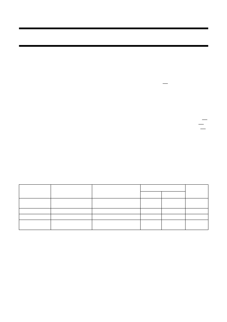
QUICK REFERENCE DATA
GND = 0 V; T
amb
= 25
°
C; t
r
= t
f
≤
3.0 ns.
Notes
1.
C
PD
is used to determine the dynamic power dissipation (P
D
in
μ
W).
P
D
= C
PD
×
V
CC2
×
f
i
+
∑
(C
L
×
V
CC2
×
f
o
) where:
f
i
= input frequency in MHz;
f
o
= output frequency in MHz;
∑
(C
L
×
V
CC2
×
f
o
) = sum of outputs;
C
L
= output load capacitance in pF;
V
CC
= supply voltage in Volts.
The condition is V
I
= GND to V
CC
.
2.
SYMBOL
PARAMETER
CONDITIONS
TYPICAL
UNIT
AHC
AHCT
t
PHL
/t
PLH
propagation delay
D
n
to Q
n
; LE to Q
n
input capacitance
output capacitance
power dissipation
capacitance
C
L
= 15 pF; V
CC
= 5 V
4.2
3.9
ns
C
I
C
O
C
PD
V
I
= V
CC
or GND
3.0
4.0
12
3.0
4.0
18
pF
pF
pF
C
L
= 50 pF; f = 1 MHz;
notes 1 and 2
相關(guān)PDF資料 |
PDF描述 |
|---|---|
| 7C33128PFS36A | 3.3V 128K x 32/36 pipeline burst synchronous SRAM |
| 7C | MCU CMOS 8 LD 1K FLASH, -40C to +85C, 8-SOIC 150mil, TUBE |
| 7HCPL-5230-200 | Hermetically Sealed, Low IF, Wide VCC, Logic Gate Optocouplers |
| 7HCT1284D | Parallel printer interface transceiver/buffer |
| 7LN115 | Optoelectronic |
相關(guān)代理商/技術(shù)參數(shù) |
參數(shù)描述 |
|---|---|
| 7AM027A5-1079-5 | 制造商:Klixon 功能描述:THERMAL PROTECTOR |
| 7AM028A5 | 制造商:SENSATA 功能描述:THERMAL PROTECTOR |
| 7AM029A5 | 制造商:Klixon 功能描述:THERMAL PROTECTOR |
| 7AM034A5275 | 制造商:klixon 功能描述:_ |
| 7AM034A5-275 | 制造商:klixon 功能描述:_ |
發(fā)布緊急采購(gòu),3分鐘左右您將得到回復(fù)。