- 您現(xiàn)在的位置:買賣IC網(wǎng) > PDF目錄360546 > 7ABT2952PWDH (NXP Semiconductors N.V.) Octal registered transceiver 3-State PDF資料下載
參數(shù)資料
| 型號: | 7ABT2952PWDH |
| 廠商: | NXP Semiconductors N.V. |
| 英文描述: | Octal registered transceiver 3-State |
| 中文描述: | 登記收發(fā)器八路三態(tài) |
| 文件頁數(shù): | 2/12頁 |
| 文件大小: | 110K |
| 代理商: | 7ABT2952PWDH |
Philips Semiconductors
Product specification
74ABT2952
Octal registered transceiver (3-State)
2
1998 Feb 11
853-1554 18949
FEATURES
8-bit registered transceiver
Independent registers for A and B buses
Output capability: +64mA/–32mA
Latch-up protection exceeds 500mA per JEDEC Std 17
ESD protection exceeds 2000V per MIL STD 883 Method 3015
and 200V per Machine Model
Power-up 3-State
Power-up reset
Live insertion/extraction permitted
DESCRIPTION
The 74ABT2952 high-performance BiCMOS device combines low
static and dynamic power dissipation with high speed and high
output drive.
The 74ABT2952 device is an 8-bit registered transceiver. Two 8-bit
back-to-back registers store data flowing in both directions between
two bidirectional buses. Data applied to the inputs is entered and
stored on the rising edge of the Clock (CPXX) provided that the
Clock Enable (CEXX) is Low. The data is then present at the 3-State
output buffers, but is only accessible when the Output Enable
(OEXX) is Low. Data flow from A inputs to B outputs is the same as
for B inputs to A outputs.
QUICK REFERENCE DATA
SYMBOL
PARAMETER
CONDITIONS
T
amb
= 25
°
C; GND = 0V
TYPICAL
UNIT
t
PLH
t
PHL
Propagation delay
CPBA to An or
CPAB to Bn
C
L
= 50pF; V
CC
= 5V
5.7
ns
C
IN
Input capacitance
V
I
= 0V or V
CC
4
pF
C
I/O
I/O capacitance
Outputs disabled; V
O
= 0V or V
CC
7
pF
I
CCZ
Total supply current
Outputs disabled; V
CC
=5.5V
110
μ
A
ORDERING INFORMATION
PACKAGES
TEMPERATURE RANGE
OUTSIDE NORTH AMERICA
NORTH AMERICA
DWG NUMBER
24-Pin Plastic DIP
–40
°
C to +85
°
C
74ABT2952 N
74ABT2952 N
SOT222-1
24-Pin plastic SO
–40
°
C to +85
°
C
74ABT2952 D
74ABT2952 D
SOT137-1
24-Pin Plastic SSOP Type II
–40
°
C to +85
°
C
74ABT2952 DB
74ABT2952 DB
SOT340-1
24-Pin Plastic TSSOP Type I
–40
°
C to +85
°
C
74ABT2952 PW
7ABT2952PW DH
SOT355-1
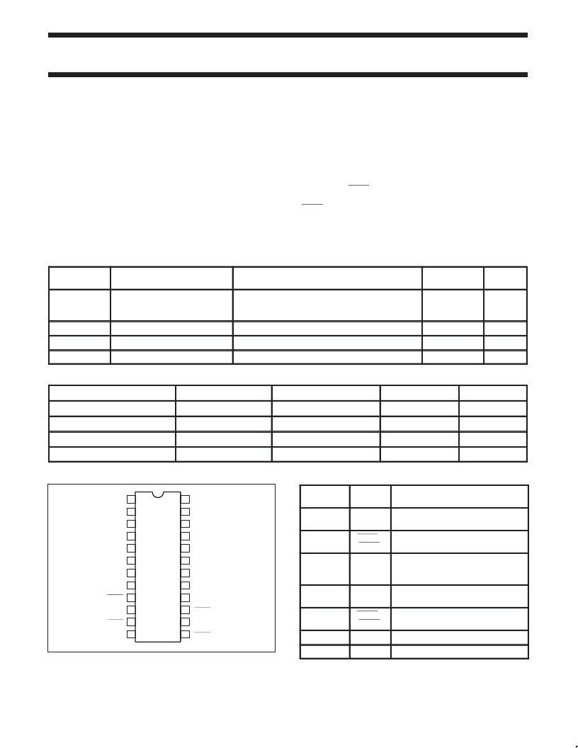
PIN CONFIGURATION
1
2
3
4
5
6
7
8
9
10
15
16
17
18
19
20
21
22
23
24
B7
B6
B5
B4
B3
B2
B1
B0
OEAB
A0
CPAB
A1
A2
A3
A4
A5
A6
A7
V
CC
OEBA
11
14
CEAB
CPBA
12
13
GND
CEBA
SA00114
PIN DESCRIPTION
PIN
NUMBER
SYMBOL
NAME AND FUNCTION
10, 14
CPAB /
CPBA
Clock input A to B / Clock input B to A
11, 13
CEAB /
CEBA
Clock enable input A to B / Clock
enable input B to A
16, 17, 18,
19, 20, 21,
22, 23
A0 – A7
Data inputs/outputs (A side)
1, 2, 3, 4, 5,
6, 7, 8
B0 – B7
Data outputs/outputs (B side)
9, 15
OEAB /
OEBA
Output enable inputs
12
GND
Ground (0V)
24
V
CC
Positive supply voltage
相關(guān)PDF資料 |
PDF描述 |
|---|---|
| 7ABT373APWDH | Octal transparent latch 3-State |
| 7ABT543APWDH | Octal latched transceiver with dual enable 3-State |
| 7ABT574APWDH | Octal D-type flip-flop 3-State |
| 7ABT646APWDH | Octal bus transceiver/register 3-State |
| 7AHCT125PWDH | SW PUSHBUTTON HERMETCALLY SEAL |
相關(guān)代理商/技術(shù)參數(shù) |
參數(shù)描述 |
|---|---|
| 7ABT373APWDH | 制造商:PHILIPS 制造商全稱:NXP Semiconductors 功能描述:Octal transparent latch 3-State |
| 7ABT543APWDH | 制造商:PHILIPS 制造商全稱:NXP Semiconductors 功能描述:Octal latched transceiver with dual enable 3-State |
| 7ABT574APWDH | 制造商:PHILIPS 制造商全稱:NXP Semiconductors 功能描述:Octal D-type flip-flop 3-State |
| 7ABT646APWDH | 制造商:PHILIPS 制造商全稱:NXP Semiconductors 功能描述:Octal bus transceiver/register 3-State |
| 7AC12 | 功能描述:基本/快動開關(guān) SUBMINIATURE BASICS RoHS:否 制造商:Omron Electronics 觸點(diǎn)形式:SPDT 執(zhí)行器:Lever 電流額定值:5 A 電壓額定值 AC:250 V 電壓額定值 DC:30 V 功率額定值: 工作力:120 g IP 等級:IP 67 NEMA 額定值: 端接類型:Wire 安裝:Panel |
發(fā)布緊急采購,3分鐘左右您將得到回復(fù)。