- 您現(xiàn)在的位置:買賣IC網(wǎng) > PDF目錄360505 > 74LVT646 (NXP Semiconductors N.V.) 3.3V Octal bus transceiver/register 3-State PDF資料下載
參數(shù)資料
| 型號(hào): | 74LVT646 |
| 廠商: | NXP Semiconductors N.V. |
| 英文描述: | 3.3V Octal bus transceiver/register 3-State |
| 中文描述: | 3.3V的八路總線收發(fā)器/寄存器三態(tài) |
| 文件頁數(shù): | 2/14頁 |
| 文件大小: | 109K |
| 代理商: | 74LVT646 |
Philips Semiconductors
Product specification
74LVT646
3.3V Octal bus transceiver/register (3-State)
2
1998 Feb 19
853-1747 18987
FEATURES
Combines 74LVT245 and 74LVT574 type functions in one device
Independent registers for A and B buses
Multiplexed real–time and stored data
Output capability: +64mA/–32mA
TTL input and output switching levels
Input and output interface capability to systems at 5V supply
Bus-hold data inputs eliminate the need for external pull-up
resistors to hold unused inputs
Live insertion/extraction permitted
No bus current loading when output is tied to 5V bus
Latch-up protection exceeds 500mA per JEDEC Std 17
Power-up 3-State
Power-up reset
ESD protection exceeds 2000V per MIL STD 883 Method 3015
and 200V per Machine Model
DESCRIPTION
The LVT646 is a high-performance BiCMOS product designed for
V
CC
operation at 3.3V.
This device consists of bus transceiver circuits with 3-State outputs,
D-type flip-flops, and control circuitry arranged for multiplexed
transmission of data directly from the input bus or the internal
registers.
Data on the A or B bus will be clocked into the registers as the
appropriate clock pin goes High.
Output Enable (OE) and DIR pins are provided to control the
transceiver function. In the transceiver mode, data present at the
high impedance port may be stored in either the A or B register or
both.
The Select (SAB, SBA) pins determine whether data is stored or
transferred through the device in real–time. The DIR determines
which bus will receive data when the OE is active (Low).
In the isolation mode (OE = High), data from Bus A may be stored in
the B register and/or data from Bus B may be stored in the A
register.
When an output function is disabled, the input function is still
enabled and may be used to store and transmit data. Only one of
the two buses, A or B may be driven at a time. The examples on the
next page demonstrate the four fundamental bus management
functions that can be performed with the 74LVT646.
QUICK REFERENCE DATA
SYMBOL
PARAMETER
CONDITIONS
T
amb
= 25
°
C; GND = 0V
TYPICAL
UNIT
t
PLH
t
PHL
Propagation delay
An to Bn or Bn to An
C
L
= 50pF; V
CC
= 3.3V
2.8
2.7
ns
C
IN
Input capacitance
CP, S, OE, DIR
V
I/O
= 0V or 3.0V
4
pF
C
I/O
I
CCZ
I/O capacitance
Total supply current
Outputs disabled; V
I/O
= 0V or 3.0V
Outputs disabled; V
CC
= 3.6V
10
0.13
pF
mA
ORDERING INFORMATION
PACKAGES
24-Pin Plastic SOL
24-Pin Plastic SSOP Type II
24-Pin Plastic TSSOP Type I
TEMPERATURE RANGE
–40
°
C to +85
°
C
–40
°
C to +85
°
C
–40
°
C to +85
°
C
OUTSIDE NORTH AMERICA
74LVT646 D
74LVT646 DB
74LVT646 PW
NORTH AMERICA
74LVT646 D
74LVT646 DB
74LVT646PW DH
DWG NUMBER
SOT163-1
SOT399-1
SOT360-1
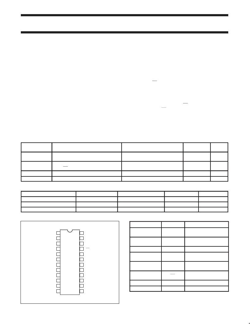
PIN CONFIGURATION
V
CC
CPBA
SBA
OE
B0
B1
B2
B3
B4
B5
B6
B7
CPAB
SAB
DIR
A0
A1
A2
A3
A4
A5
A6
A7
GND
24
23
22
21
20
19
18
17
16
15
14
13
1
2
3
4
5
6
7
8
9
10
11
12
SV00045
PIN DESCRIPTION
PIN NUMBER
SYMBOL
FUNCTION
1, 23
CPAB /
CPBA
A to B clock input / B to A
clock input
2, 22
SAB / SBA
A to B select input / B to
A select input
3
DIR
Direction control input
4, 5, 6, 7, 8, 9, 10,
11
A0 – A7
Data inputs/outputs (A
side)
20, 19, 18, 17, 16,
15, 14, 13
B0 – B7
Data inputs/outputs (B
side)
21
OE
Output enable input
(active-low)
12
GND
Ground (0V)
24
V
CC
Positive supply voltage
相關(guān)PDF資料 |
PDF描述 |
|---|---|
| 74LVT646PWDH | 3.3V Octal bus transceiver/register 3-State |
| 74LVT652 | 3.3V Octal transceiver/register, non-inverting 3-State |
| 74LVT652PWDH | 3.3V Octal transceiver/register, non-inverting 3-State |
| 74LVT74 | 3.3V Dual D-type flip-flop |
| 74LVT74PWDH | 8-Bit Shift Registers With Output Registers 16-PDIP -40 to 85 |
相關(guān)代理商/技術(shù)參數(shù) |
參數(shù)描述 |
|---|---|
| 74LVT646D | 功能描述:總線收發(fā)器 3.3V OCTAL REG XCVR 3-S RoHS:否 制造商:Fairchild Semiconductor 邏輯類型:CMOS 邏輯系列:74VCX 每芯片的通道數(shù)量:16 輸入電平:CMOS 輸出電平:CMOS 輸出類型:3-State 高電平輸出電流:- 24 mA 低電平輸出電流:24 mA 傳播延遲時(shí)間:6.2 ns 電源電壓-最大:2.7 V, 3.6 V 電源電壓-最小:1.65 V, 2.3 V 最大工作溫度:+ 85 C 封裝 / 箱體:TSSOP-48 封裝:Reel |
| 74LVT646D,112 | 功能描述:總線收發(fā)器 3.3V OCTAL REG XCVR RoHS:否 制造商:Fairchild Semiconductor 邏輯類型:CMOS 邏輯系列:74VCX 每芯片的通道數(shù)量:16 輸入電平:CMOS 輸出電平:CMOS 輸出類型:3-State 高電平輸出電流:- 24 mA 低電平輸出電流:24 mA 傳播延遲時(shí)間:6.2 ns 電源電壓-最大:2.7 V, 3.6 V 電源電壓-最小:1.65 V, 2.3 V 最大工作溫度:+ 85 C 封裝 / 箱體:TSSOP-48 封裝:Reel |
| 74LVT646D,118 | 功能描述:總線收發(fā)器 3.3V OCTAL REG XCVR RoHS:否 制造商:Fairchild Semiconductor 邏輯類型:CMOS 邏輯系列:74VCX 每芯片的通道數(shù)量:16 輸入電平:CMOS 輸出電平:CMOS 輸出類型:3-State 高電平輸出電流:- 24 mA 低電平輸出電流:24 mA 傳播延遲時(shí)間:6.2 ns 電源電壓-最大:2.7 V, 3.6 V 電源電壓-最小:1.65 V, 2.3 V 最大工作溫度:+ 85 C 封裝 / 箱體:TSSOP-48 封裝:Reel |
| 74LVT646DB | 功能描述:總線收發(fā)器 3.3V OCTAL REG XCVR 3-S RoHS:否 制造商:Fairchild Semiconductor 邏輯類型:CMOS 邏輯系列:74VCX 每芯片的通道數(shù)量:16 輸入電平:CMOS 輸出電平:CMOS 輸出類型:3-State 高電平輸出電流:- 24 mA 低電平輸出電流:24 mA 傳播延遲時(shí)間:6.2 ns 電源電壓-最大:2.7 V, 3.6 V 電源電壓-最小:1.65 V, 2.3 V 最大工作溫度:+ 85 C 封裝 / 箱體:TSSOP-48 封裝:Reel |
| 74LVT646DB,112 | 功能描述:總線收發(fā)器 3.3V OCTAL REG XCVR RoHS:否 制造商:Fairchild Semiconductor 邏輯類型:CMOS 邏輯系列:74VCX 每芯片的通道數(shù)量:16 輸入電平:CMOS 輸出電平:CMOS 輸出類型:3-State 高電平輸出電流:- 24 mA 低電平輸出電流:24 mA 傳播延遲時(shí)間:6.2 ns 電源電壓-最大:2.7 V, 3.6 V 電源電壓-最小:1.65 V, 2.3 V 最大工作溫度:+ 85 C 封裝 / 箱體:TSSOP-48 封裝:Reel |
發(fā)布緊急采購,3分鐘左右您將得到回復(fù)。