- 您現(xiàn)在的位置:買賣IC網(wǎng) > PDF目錄360488 > 74LV423PWDH (NXP SEMICONDUCTORS) Dual retriggerable monostable multivibrator with reset PDF資料下載
參數(shù)資料
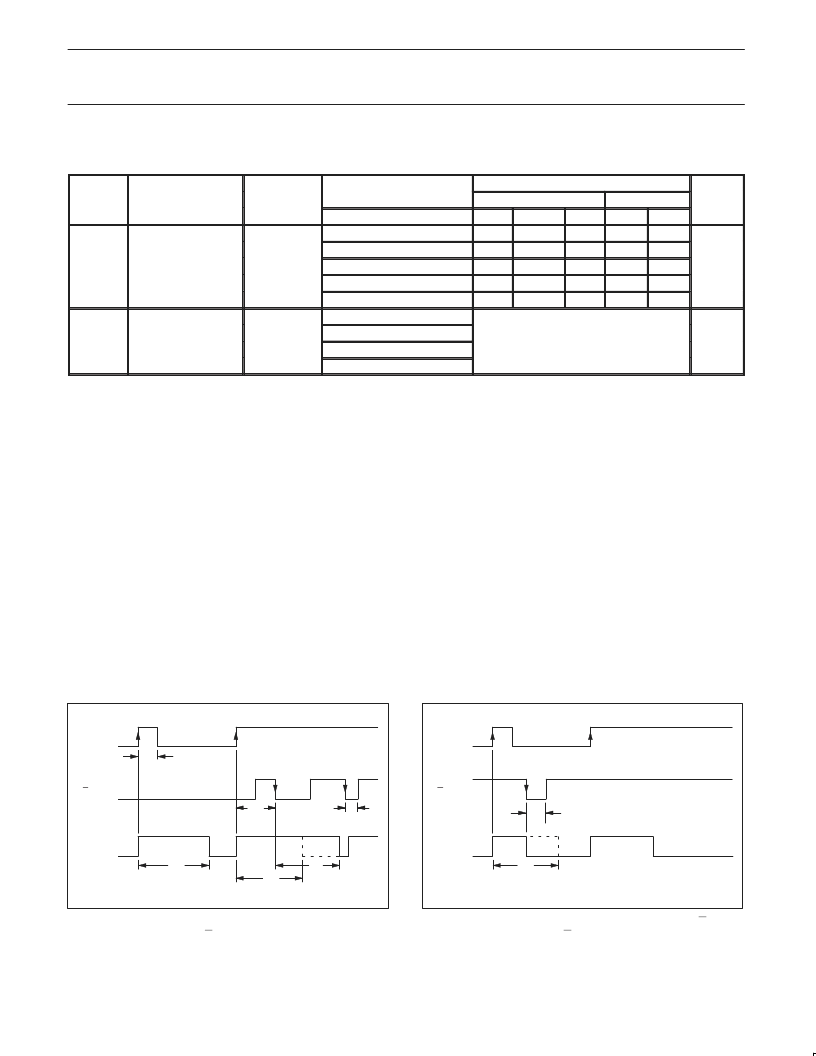
| 型號(hào): | 74LV423PWDH |
| 廠商: | NXP SEMICONDUCTORS |
| 元件分類: | 諧振器 |
| 英文描述: | Dual retriggerable monostable multivibrator with reset |
| 中文描述: | LV/LV-A/LVX/H SERIES, DUAL MONOSTABLE MULTIVIBRATOR, PDSO16 |
| 封裝: | PLASTIC, TSSOP1-16 |
| 文件頁(yè)數(shù): | 8/16頁(yè) |
| 文件大?。?/td> | 156K |
| 代理商: | 74LV423PWDH |
第1頁(yè)第2頁(yè)第3頁(yè)第4頁(yè)第5頁(yè)第6頁(yè)第7頁(yè)當(dāng)前第8頁(yè)第9頁(yè)第10頁(yè)第11頁(yè)第12頁(yè)第13頁(yè)第14頁(yè)第15頁(yè)第16頁(yè)
Philips Semiconductors
Preliminary specification
74LV423
Dual retriggerable monostable multivibrator
with reset
1997 Feb 04
8
AC CHARACTERISTICS
(Continued)
GND = 0V; t
r
= t
f
≤
2.5ns; C
L
= 50pF; R
L
= 1K
CONDITION
LIMITS
SYMBOL
PARAMETER
WAVEFORM
–40 to +85
°
C
TYP
1
–40 to +125
°
C
MIN
UNIT
V
CC
(V)
1.2
2.0
2.7
3.0 to 3.6
4.5 to 5.5
2.0
2.7
3.0 to 3.6
4.5 to 5.5
MIN
20
5
5
2
2
MAX
1000
1000
1000
1000
1000
MAX
External timing
resistor
R
EXT
Figure 6
k
C
EXT
External timing
capacitor
Figure 6
3
No limits
pF
g
NOTES:
1. Unless otherwise stated, all typical values are at T
amb
= 25
°
C.
2. Typical value measured at V
CC
= 3.3V.
3. Typical value measured at V
CC
= 5.0V.
4. For other R
EXT
and C
EXT
combinations see Figure 6.
if C
EXT
> 10 nF, the next formula is valid:
t
W
= K x R
EXT
x C
EXT
(typ.)
where, t
W
= output pulse width in ns;
R
EXT
= external resistor in k
; C
= external capacitor in pF;
K
= constant = 0.45 for V
= 5.0V and 0.48 for V
CC
= 2.0V.
The inherent test jig and pin capacitance at pins 15 and 7 (nR
EXT
/C
EXT
) is approximately 7 pF.
5. The time to retrigger the monostable multivibrator depends on the values of R
EXT
and C
EXT
.
The output pulse width will only be extended when the time between the active-going edges of the
trigger pulses meets the minimum retrigger time.
If C
EXT
> 10 pF, the next formula (at V
CC
= 5.0V) for the set-up time of a retrigger pulse is valid:
t
rt
= 30 + 0.19R x C
-9
+ 13 x R
1.05
(typ.)
where, t
rt
= retrigger time in ns;
C
EXT
= external capacitor in pF;
R
= external resistor in k
.
The inherent test jig and pin capacitance at pins 15 and 7 (nR
EXT
/C
EXT
) is approximately 7 pF.
6. When the device is powered up, initiate the device via a reset pulse, when C
EXT
< 50pF.
AC WAVEFORMS
V
M
= 1.5V at V
CC
V
and V
are the typical output voltage drop that occur
with the output load.
2.7V; V
M
= 0.5 V
CC
at V
CC
2.7V.
t
W
t
W
t
rt
t
W
t
W
t
W
nB INPUT
nA INPUT
nQ OUTPUT
SV00139
Figure 2. Output pulse control using retrigger pulse;
nR
D
= HIGH.
t
W
t
W
nB INPUT
nR
D
INPUT
nQ OUTPUT
SV00164
Figure 3. Output pulse control using reset input nR
D
;
nA = LOW.
相關(guān)PDF資料 |
PDF描述 |
|---|---|
| 74LV423 | Dual retriggerable monostable multivibrator with reset |
| 74LV4316PW-T | SPST Analog Switch |
| 74LV4799DB-T | 8K, 1K X 8 1.8V SERIAL EE, IND, -40C to +85C, 8-MSOP, TUBE |
| 74LV4799D-T | 8K, 1K X 8 1.8V SERIAL EE, -40C to +85C, 8-PDIP, TUBE |
| 74LV4799PW-T | 8K, 1K X 8 2.5V SERIAL EE, -40C to +85C, 8-PDIP, TUBE |
相關(guān)代理商/技術(shù)參數(shù) |
參數(shù)描述 |
|---|---|
| 74LV4316 | 制造商:PHILIPS 制造商全稱:NXP Semiconductors 功能描述:Quad bilateral switches |
| 74LV4316D | 制造商:PHILIPS 制造商全稱:NXP Semiconductors 功能描述:Quad bilateral switches |
| 74LV4316DB | 制造商:PHILIPS 制造商全稱:NXP Semiconductors 功能描述:Quad bilateral switches |
| 74LV4316DB-T | 制造商:未知廠家 制造商全稱:未知廠家 功能描述:SPST Analog Switch |
| 74LV4316D-T | 制造商:未知廠家 制造商全稱:未知廠家 功能描述:SPST Analog Switch |
發(fā)布緊急采購(gòu),3分鐘左右您將得到回復(fù)。