- 您現(xiàn)在的位置:買賣IC網(wǎng) > PDF目錄360483 > 74LV03PWDH (NXP SEMICONDUCTORS) Quad 2-input NAND gate PDF資料下載
參數(shù)資料
| 型號: | 74LV03PWDH |
| 廠商: | NXP SEMICONDUCTORS |
| 元件分類: | 通用總線功能 |
| 英文描述: | Quad 2-input NAND gate |
| 中文描述: | LV/LV-A/LVX/H SERIES, QUAD 2-INPUT NAND GATE, PDSO14 |
| 文件頁數(shù): | 4/12頁 |
| 文件大小: | 119K |
| 代理商: | 74LV03PWDH |
Philips Semiconductors
Product specification
74LV03
Quad 2-input NAND gate
1998 Apr 20
4
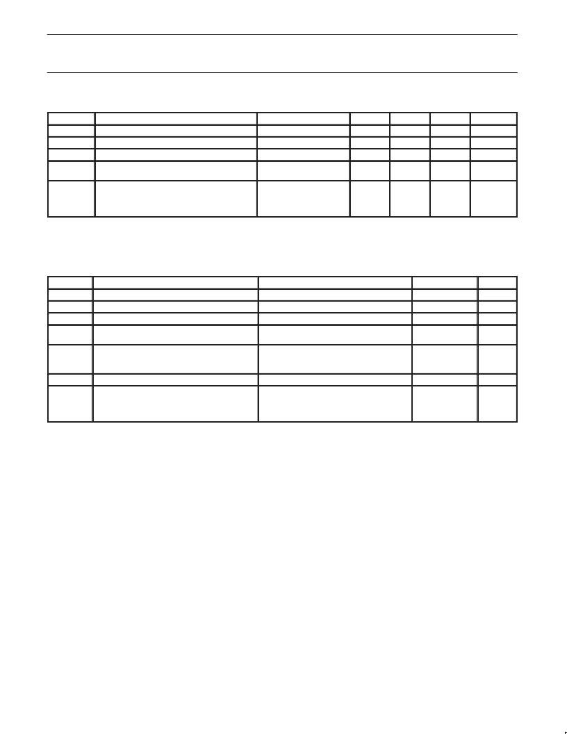
RECOMMENDED OPERATING CONDITIONS
SYMBOL
V
CC
DC supply voltage
V
I
Input voltage
V
O
Output voltage
Operating ambient temperature range in free
air
PARAMETER
CONDITIONS
See Note1
MIN
1.0
0
0
–40
–40
TYP.
3.3
–
–
MAX
5.5
V
CC
V
CC
+85
+125
500
200
100
50
UNIT
V
V
V
T
amb
See DC and AC
characteristics
V
CC
= 1.0V to 2.0V
V
CC
= 2.0V to 2.7V
V
CC
= 2.7V to 3.6V
V
CC
= 3.6V to 5.5V
°
C
t
r
, t
f
Input rise and fall times
–
–
–
–
–
–
–
ns/V
NOTES:
1
The LV is guaranteed to function down to V
CC
= 1.0V (input levels GND or V
CC
); DC characteristics are guaranteed from V
CC
= 1.2V to V
CC
= 5.5V.
ABSOLUTE MAXIMUM RATINGS
1, 2
In accordance with the Absolute Maximum Rating System (IEC 134)
Voltages are referenced to GND (ground = 0V)
SYMBOL
PARAMETER
V
CC
DC supply voltage
±
I
IK
DC input diode current
±
I
OK
DC output diode current
DC output source or sink current
– standard outputs
CONDITIONS
RATING
–0.5 to +7.0
20
50
UNIT
V
mA
mA
V
I
< –0.5 or V
I
> V
CC
+ 0.5V
V
O
< –0.5 or V
O
> V
CC
+ 0.5V
±
I
O
–0.5V < V
O
< V
CC
+ 0.5V
25
mA
±
I
GND
,
±
I
CC
T
stg
DC V
CC
or GND current for types with
–standard outputs
50
mA
Storage temperature range
Power dissipation per package
–plastic DIL
–plastic mini-pack (SO)
–plastic shrink mini-pack (SSOP and TSSOP)
–65 to +150
°
C
P
TOT
for temperature range: –40 to +125
°
C
above +70
°
C derate linearly with 12mW/K
above +70
°
C derate linearly with 8 mW/K
above +60
°
C derate linearly with 5.5 mW/K
750
500
400
mW
NOTES:
1
Stresses beyond those listed may cause permanent damage to the device. These are stress ratings only and functional operation of the
device at these or any other conditions beyond those indicated under “recommended operating conditions” is not implied. Exposure to
absolute-maximum-rated conditions for extended periods may affect device reliability.
2
The input and output voltage ratings may be exceeded if the input and output current ratings are observed.
相關(guān)PDF資料 |
PDF描述 |
|---|---|
| 74LV04PWDH | CERAMIC CHIP/MIL-PRF-55681 |
| 74LV04 | CERAMIC CHIP/MIL-PRF-55681 |
| 74LV08PWDH | Quad 2-input AND gate |
| 74LV08 | Quad 2-input AND gate |
| 74LV107DB-T | J-K-Type Flip-Flop |
相關(guān)代理商/技術(shù)參數(shù) |
參數(shù)描述 |
|---|---|
| 74LV03PW-T | 制造商:未知廠家 制造商全稱:未知廠家 功能描述:Quad 2-input NAND Gate |
| 74LV04 | 制造商:PHILIPS 制造商全稱:NXP Semiconductors 功能描述:Hex inverter |
| 74LV0451D | 制造商:未知廠家 制造商全稱:未知廠家 功能描述:Interface IC |
| 74LV0451N | 制造商:未知廠家 制造商全稱:未知廠家 功能描述:Interface IC |
| 74LV04A | 制造商:TI 制造商全稱:Texas Instruments 功能描述:HEX INVERTERS |
發(fā)布緊急采購,3分鐘左右您將得到回復(fù)。