- 您現(xiàn)在的位置:買賣IC網(wǎng) > PDF目錄360461 > 74HCT533 (NXP Semiconductors N.V.) CONNECTOR ACCESSORY PDF資料下載
參數(shù)資料
| 型號(hào): | 74HCT533 |
| 廠商: | NXP Semiconductors N.V. |
| 英文描述: | CONNECTOR ACCESSORY |
| 中文描述: | 連接器附件 |
| 文件頁數(shù): | 2/7頁 |
| 文件大小: | 62K |
| 代理商: | 74HCT533 |
December 1990
2
Philips Semiconductors
Product specification
Octal D-type transparent latch; 3-state;
inverting
74HC/HCT533
FEATURES
3-state inverting outputs for bus oriented applications
Common 3-state output enable input
Output capability: bus driver
I
CC
category: MSI
GENERAL DESCRIPTION
The 74HC/HCT533 are high-speed Si-gate CMOS devices
and are pin compatible with low power Schottky TTL
(LSTTL). They are specified in compliance with JEDEC
standard no. 7A.
The 74HC/HCT533 are octal D-type transparent latches
featuring separate D-type inputs for each latch and 3-state
outputs for bus oriented applications. A latch enable (LE)
input and an output enable (OE) input are common to all
latches.
The “533” consists of eight D-type transparent latches with
3-state inverting outputs. When LE is HIGH, data at the D
n
inputs enter the latches. In this condition the latches are
transparent, i.e. a latch output will change state each time
its corresponding D-input changes.
When LE is LOW the latches store the information that was
present at the D-inputs a set-up time preceding the
HIGH-to-LOW transition of LE.
When OE is LOW, the contents of the 8 latches are
available at the outputs.
When OE is HIGH, the outputs go to the high impedance
OFF-state. Operation of the OE input does not affect the
state of the latches.
The “533” is functionally identical to the “373”, “563” and
“573”, but the “373” and “573” have non-inverted outputs
and the “563” and “573” have a different pin arrangement.
QUICK REFERENCE DATA
GND = 0 V; T
amb
= 25
°
C; t
r
= t
f
= 6 ns
Notes
1.
C
PD
is used to determine the dynamic power dissipation (P
D
in
μ
W):
P
D
= C
PD
×
V
CC2
×
f
i
+ ∑
(C
L
×
V
CC2
×
f
o
) where:
f
i
= input frequency in MHz
f
o
= output frequency in MHz
∑
(C
L
×
V
CC2
×
f
o
) = sum of outputs
C
L
= output load capacitance in pF
V
CC
= supply voltage in V
For HC the condition is V
I
= GND to V
CC
For HCT the condition is V
I
= GND to V
CC
1.5 V
2.
ORDERING INFORMATION
See
“74HC/HCT/HCU/HCMOS Logic Package Information”
.
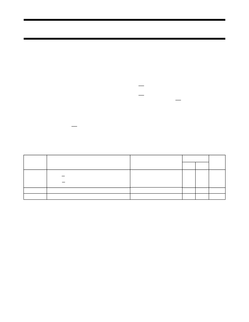
SYMBOL
PARAMETER
CONDITIONS
TYPICAL
UNIT
HC
HCT
t
PHL/
t
PLH
propagation delay
D
n
to Q
n
LE to Q
n
input capacitance
power dissipation capacitance per latch
C
L
= 15 pF; V
CC
= 5 V
14
18
3.5
34
16
19
3.5
34
ns
ns
pF
pF
C
I
C
PD
notes 1 and 2
相關(guān)PDF資料 |
PDF描述 |
|---|---|
| 74HC58 | Dual AND-OR gate(雙與或門) |
| 74HC594 | 8-bit shift register with output register |
| 74HCT594 | 4-Bit Synchronous Up/Down Counters (Dual Clock With Clear) 16-TSSOP -40 to 85 |
| 74HC595 | 8-bit serial-in/serial or parallel-out shift register with output latches; 3-state |
| 74HCT595 | 4-Bit Synchronous Up/Down Counters (Dual Clock With Clear) 16-TSSOP -40 to 85 |
相關(guān)代理商/技術(shù)參數(shù) |
參數(shù)描述 |
|---|---|
| 74HCT534 | 制造商:SGS-thom 功能描述:74HCT534 |
| 74HCT534D | 功能描述:觸發(fā)器 OCTAL D INV 3-STATE RoHS:否 制造商:Texas Instruments 電路數(shù)量:2 邏輯系列:SN74 邏輯類型:D-Type Flip-Flop 極性:Inverting, Non-Inverting 輸入類型:CMOS 輸出類型: 傳播延遲時(shí)間:4.4 ns 高電平輸出電流:- 16 mA 低電平輸出電流:16 mA 電源電壓-最大:5.5 V 最大工作溫度:+ 85 C 安裝風(fēng)格:SMD/SMT 封裝 / 箱體:X2SON-8 封裝:Reel |
| 74HCT534D,652 | 功能描述:觸發(fā)器 OCTAL D INV 3-STATE RoHS:否 制造商:Texas Instruments 電路數(shù)量:2 邏輯系列:SN74 邏輯類型:D-Type Flip-Flop 極性:Inverting, Non-Inverting 輸入類型:CMOS 輸出類型: 傳播延遲時(shí)間:4.4 ns 高電平輸出電流:- 16 mA 低電平輸出電流:16 mA 電源電壓-最大:5.5 V 最大工作溫度:+ 85 C 安裝風(fēng)格:SMD/SMT 封裝 / 箱體:X2SON-8 封裝:Reel |
| 74HCT534D,653 | 功能描述:觸發(fā)器 OCTAL D INV 3-STATE RoHS:否 制造商:Texas Instruments 電路數(shù)量:2 邏輯系列:SN74 邏輯類型:D-Type Flip-Flop 極性:Inverting, Non-Inverting 輸入類型:CMOS 輸出類型: 傳播延遲時(shí)間:4.4 ns 高電平輸出電流:- 16 mA 低電平輸出電流:16 mA 電源電壓-最大:5.5 V 最大工作溫度:+ 85 C 安裝風(fēng)格:SMD/SMT 封裝 / 箱體:X2SON-8 封裝:Reel |
| 74HCT534D-T | 功能描述:觸發(fā)器 OCTAL D INV 3-STATE RoHS:否 制造商:Texas Instruments 電路數(shù)量:2 邏輯系列:SN74 邏輯類型:D-Type Flip-Flop 極性:Inverting, Non-Inverting 輸入類型:CMOS 輸出類型: 傳播延遲時(shí)間:4.4 ns 高電平輸出電流:- 16 mA 低電平輸出電流:16 mA 電源電壓-最大:5.5 V 最大工作溫度:+ 85 C 安裝風(fēng)格:SMD/SMT 封裝 / 箱體:X2SON-8 封裝:Reel |
發(fā)布緊急采購,3分鐘左右您將得到回復(fù)。