- 您現(xiàn)在的位置:買賣IC網(wǎng) > PDF目錄360472 > 74HCT4316 (NXP Semiconductors N.V.) Quad bilateral switches(四雙向開關(guān)) PDF資料下載
參數(shù)資料
| 型號: | 74HCT4316 |
| 廠商: | NXP Semiconductors N.V. |
| 英文描述: | Quad bilateral switches(四雙向開關(guān)) |
| 中文描述: | 四(四雙向開關(guān)雙邊開關(guān)) |
| 文件頁數(shù): | 2/15頁 |
| 文件大?。?/td> | 130K |
| 代理商: | 74HCT4316 |
September 1993
2
Philips Semiconductors
Product specification
Quad bilateral switches
74HC/HCT4316
FEATURES
Low “ON” resistance:
160
(typ.) at V
CC
V
EE
= 4.5 V
120
(typ.) at V
CC
V
EE
= 6.0 V
80
(typ.) at V
CC
V
EE
= 9.0 V
Logic level translation:
to enable 5 V logic to communicate
with
±
5 V analog signals
Typical “break before make” built in
Output capability: non-standard
I
CC
category: MSI
GENERAL DESCRIPTION
The 74HC/HCT4316 are high-speed Si-gate CMOS
devices. They are specified in compliance with JEDEC
standard no. 7A.
The 74HC/HCT4316 have four independent analog
switches. Each switch has two input/output terminals
(nY, nZ) and an active HIGH select input (nS). When the
enable input (E) is HIGH, all four analog switches are
turned off.
Current through a switch will not cause additional V
CC
current provided the voltage at the terminals of the switch
is maintained within the supply voltage range;
V
CC
>>
(V
Y
, V
Z
)
>>
V
EE
. Inputs nY and nZ are electrically
equivalent terminals.
V
CC
and GND are the supply voltage pins for the digital
control inputs (E and nS). The V
CC
to GND ranges are 2.0
to 10.0 V for HC and 4.5 to 5.5 V for HCT.
The analog inputs/outputs (nY and nZ) can swing between
V
CC
as a positive limit and V
EE
as a negative limit.
V
CC
V
EE
may not exceed 10.0 V.
See the “4016” for the version without logic level
translation.
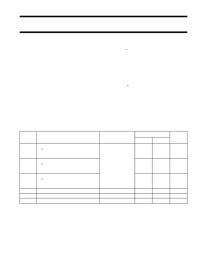
QUICK REFERENCE DATA
V
EE
= GND = 0 V; T
amb
= 25
°
C; t
r
= t
f
= 6 ns
SYMBOL
PARAMETER
CONDITIONS
TYPICAL
UNIT
HC
HCT
t
PZH
turn “ON” time
E to V
OS
nS to V
OS
turn “ON” time
E to V
OS
nS to V
OS
turn “OFF” time
E to V
OS
nS to V
OS
input capacitance
power dissipation capacitance per switch
max. switch capacitance
C
L
= 15 pF; R
L
= 1 k
;
V
CC
= 5 V
19
16
19
17
ns
ns
t
PZL
19
16
24
21
ns
ns
t
PHZ
/ t
PLZ
20
16
3.5
13
5
21
19
3.5
14
5
ns
ns
pF
pF
pF
C
I
C
PD
C
S
notes 1 and 2
Notes
1. C
PD
is used to determine the dynamic power
dissipation (P
D
in
μ
W):
P
D
= C
PD
×
V
CC2
×
f
i
+ ∑
{ (C
L
+
C
S
)
×
V
CC2
×
f
o
}
where:
f
i
= input frequency in MHz
f
o
= output frequency in MHz
∑
{ (C
L
+
C
S
)
×
V
CC2
×
f
o
} = sum of outputs
C
L
= output load capacitance in pF
C
S
= max. switch capacitance in pF
V
CC
= supply voltage in V
2. For HC the condition is V
I
= GND to V
CC
For HCT the condition is V
I
= GND to V
CC
1.5 V
相關(guān)PDF資料 |
PDF描述 |
|---|---|
| 74HC4316 | Quad bilateral switches |
| 74HCT4351 | 8-channel analog multiplexer/demultiplexer with latch(帶鎖存的8通道模擬多路復(fù)用器/多路分解器) |
| 74HC4351 | 8-channel analog multiplexer/demultiplexer with latch |
| 74HCT4352 | Quadruple D-Type Flip-Flops With Clear 16-TSSOP -40 to 85 |
| 74HC4352 | Dual 4-channel analog multiplexer/demultiplexer with latch |
相關(guān)代理商/技術(shù)參數(shù) |
參數(shù)描述 |
|---|---|
| 74HCT4316D | 功能描述:模擬開關(guān) IC QUAD BILATRL ANALOG SWITCH RoHS:否 制造商:Texas Instruments 開關(guān)數(shù)量:2 開關(guān)配置:SPDT 開啟電阻(最大值):0.1 Ohms 切換電壓(最大): 開啟時間(最大值): 關(guān)閉時間(最大值): 工作電源電壓:2.7 V to 4.5 V 最大工作溫度:+ 85 C 安裝風(fēng)格:SMD/SMT 封裝 / 箱體:DSBGA-16 |
| 74HCT4316D,112 | 功能描述:模擬開關(guān) IC QUAD BILATRL ANALOG RoHS:否 制造商:Texas Instruments 開關(guān)數(shù)量:2 開關(guān)配置:SPDT 開啟電阻(最大值):0.1 Ohms 切換電壓(最大): 開啟時間(最大值): 關(guān)閉時間(最大值): 工作電源電壓:2.7 V to 4.5 V 最大工作溫度:+ 85 C 安裝風(fēng)格:SMD/SMT 封裝 / 箱體:DSBGA-16 |
| 74HCT4316D,118 | 功能描述:模擬開關(guān) IC QUAD BILATRL ANALOG RoHS:否 制造商:Texas Instruments 開關(guān)數(shù)量:2 開關(guān)配置:SPDT 開啟電阻(最大值):0.1 Ohms 切換電壓(最大): 開啟時間(最大值): 關(guān)閉時間(最大值): 工作電源電壓:2.7 V to 4.5 V 最大工作溫度:+ 85 C 安裝風(fēng)格:SMD/SMT 封裝 / 箱體:DSBGA-16 |
| 74HCT4316DB | 功能描述:模擬開關(guān) IC QUAD BILATRL ANALOG SWITCH RoHS:否 制造商:Texas Instruments 開關(guān)數(shù)量:2 開關(guān)配置:SPDT 開啟電阻(最大值):0.1 Ohms 切換電壓(最大): 開啟時間(最大值): 關(guān)閉時間(最大值): 工作電源電壓:2.7 V to 4.5 V 最大工作溫度:+ 85 C 安裝風(fēng)格:SMD/SMT 封裝 / 箱體:DSBGA-16 |
| 74HCT4316DB,112 | 功能描述:模擬開關(guān) IC QUAD BILATRL ANALOG RoHS:否 制造商:Texas Instruments 開關(guān)數(shù)量:2 開關(guān)配置:SPDT 開啟電阻(最大值):0.1 Ohms 切換電壓(最大): 開啟時間(最大值): 關(guān)閉時間(最大值): 工作電源電壓:2.7 V to 4.5 V 最大工作溫度:+ 85 C 安裝風(fēng)格:SMD/SMT 封裝 / 箱體:DSBGA-16 |
發(fā)布緊急采購,3分鐘左右您將得到回復(fù)。