- 您現(xiàn)在的位置:買賣IC網(wǎng) > PDF目錄360471 > 74HC40105 (NXP Semiconductors N.V.) 4-bit x 16-word FIFO register PDF資料下載
參數(shù)資料
| 型號: | 74HC40105 |
| 廠商: | NXP Semiconductors N.V. |
| 英文描述: | 4-bit x 16-word FIFO register |
| 中文描述: | 4位× 16字FIFO寄存器 |
| 文件頁數(shù): | 18/25頁 |
| 文件大小: | 200K |
| 代理商: | 74HC40105 |
1998 Jan 23
18
Philips Semiconductors
Product specification
4-bit x 16-word FIFO register
74HC/HCT40105
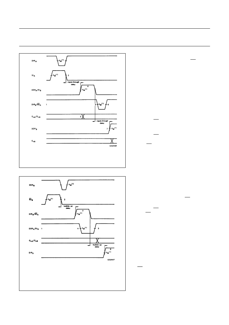
Fig.20 FIFO to FIFO communication; input timing under
empty condition.
(1) HC : V
M
= 50%; V
I
= GND to V
.
HCT : V
M
= 1.3 V; V
I
= GND to 3 V.
Notes to
Fig.20
1.
FIFO
A
and FIFO
B
initially empty, SO
A
held
HIGH in anticipation of data.
Load one word into FIFO
A
; SI pulse applied,
results in DIR pulse.
Data out
A
/data in
B
transition; valid data
arrives at FIFO
A
output stage after a specified
delay of the DOR flag, meeting data input
set-up requirements of FIFO
B
.
DOR
A
and SI
B
pulse HIGH; (ripple through
delay after SI
A
LOW) data is unloaded from
FIFO
A
as a result of the data output ready
pulse, data is shifted into FIFO
B
.
DIR
B
and SO
A
go LOW; flag indicates input
stage of FIFO
B
is busy, shift-out of FIFO
A
is
complete.
DIR
B
and SO
A
go HIGH automatically; the
input stage of FIFO
B
is again able to receive
data, SO is held HIGH in anticipation of
additional data.
DOR
B
goes HIGH; (ripple through delay after
SI
B
LOW) valid data is present one
propagation delay later at the FIFO
B
output
stage.
2.
3.
4.
5.
6.
7.
(1) HC : V
M
= 50%; V
I
= GND to V
.
HCT : V
M
= 1.3 V; V
I
= GND to 3 V.
Fig.21 FIFO to FIFO communication; output timing under
full condition.
Notes to
Fig.21
1.
FIFO
A
and FIFO
B
initially empty, SI
B
held
HIGH in anticipation of shifting in new data as
empty location bubbles-up.
Unload one word into FIFO
B
; SO pulse
applied, results in DOR pulse.
DIR
B
and SO
A
pulse HIGH; (bubble-up delay
after SO
B
LOW) data is loaded into FIFO
B
as
a result of the DIR pulse, data is shifted out of
FIFO
A
.
DOR
A
and SI
B
go LOW; flag indicates the
output stage of FIFO
A
is busy, shift-in to
FIFO
R
is complete.
DOR
A
and SI
B
go HIGH; flag indicates valid
data is again available at FIFO
A
output stage,
SI
B
is held HIGH, awaiting bubble-up of
empty location.
DIR
A
goes HIGH; (bubble-up delay after
SO
A
LOW) an empty location is present at
input stage of FIFO
A
.
2.
3.
4.
5.
6.
相關(guān)PDF資料 |
PDF描述 |
|---|---|
| 74HCT4015 | 8-Bit Parallel-Load Shift Registers 16-SO -40 to 85 |
| 74HC4015 | Dual 4-bit serial-in/parallel-out shift register |
| 74HCT4016 | Quad bilateral switches(四雙向開關(guān)) |
| 74HC4016 | Quad bilateral switches |
| 74HC4016DB | Quad bilateral switches |
相關(guān)代理商/技術(shù)參數(shù) |
參數(shù)描述 |
|---|---|
| 74HC40105D | 功能描述:寄存器 4BX16W FIFO REGISTER RoHS:否 制造商:NXP Semiconductors 邏輯類型:CMOS 邏輯系列:HC 電路數(shù)量:1 最大時鐘頻率:36 MHz 傳播延遲時間: 高電平輸出電流:- 7.8 mA 低電平輸出電流:7.8 mA 電源電壓-最大:6 V 最大工作溫度:+ 125 C 封裝 / 箱體:SOT-38 封裝:Tube |
| 74HC40105D,652 | 功能描述:寄存器 4BX16W FIFO REGISTER RoHS:否 制造商:NXP Semiconductors 邏輯類型:CMOS 邏輯系列:HC 電路數(shù)量:1 最大時鐘頻率:36 MHz 傳播延遲時間: 高電平輸出電流:- 7.8 mA 低電平輸出電流:7.8 mA 電源電壓-最大:6 V 最大工作溫度:+ 125 C 封裝 / 箱體:SOT-38 封裝:Tube |
| 74HC40105D,653 | 功能描述:寄存器 4-BIT X 16 WORD FIFO REGISTER RoHS:否 制造商:NXP Semiconductors 邏輯類型:CMOS 邏輯系列:HC 電路數(shù)量:1 最大時鐘頻率:36 MHz 傳播延遲時間: 高電平輸出電流:- 7.8 mA 低電平輸出電流:7.8 mA 電源電壓-最大:6 V 最大工作溫度:+ 125 C 封裝 / 箱體:SOT-38 封裝:Tube |
| 74HC40105D652 | 制造商:Rochester Electronics LLC 功能描述: 制造商:NXP 功能描述: 制造商:NXP Semiconductors 功能描述: |
| 74HC40105DB | 功能描述:寄存器 4-BIT X 16 WORD FIFO REGISTER RoHS:否 制造商:NXP Semiconductors 邏輯類型:CMOS 邏輯系列:HC 電路數(shù)量:1 最大時鐘頻率:36 MHz 傳播延遲時間: 高電平輸出電流:- 7.8 mA 低電平輸出電流:7.8 mA 電源電壓-最大:6 V 最大工作溫度:+ 125 C 封裝 / 箱體:SOT-38 封裝:Tube |
發(fā)布緊急采購,3分鐘左右您將得到回復(fù)。