- 您現在的位置:買賣IC網 > PDF目錄370126 > 74F413PC (FAIRCHILD SEMICONDUCTOR CORP) 64 x 4 First-In First-Out Buffer Memory with Parallel I/O PDF資料下載
參數資料
| 型號: | 74F413PC |
| 廠商: | FAIRCHILD SEMICONDUCTOR CORP |
| 元件分類: | DRAM |
| 英文描述: | 64 x 4 First-In First-Out Buffer Memory with Parallel I/O |
| 中文描述: | 64 X 4 OTHER FIFO, 55 ns, PDIP16 |
| 封裝: | 0.300 INCH, PLASTIC, MS-001, DIP-16 |
| 文件頁數: | 2/6頁 |
| 文件大小: | 113K |
| 代理商: | 74F413PC |

Unit Loading/Fan Out
54F/74F
Pin Names
Description
U.L.
Input I
IH
/I
IL
Output I
OH
/I
OL
HIGH/LOW
D
0
–D
3
O
0
–O
3
IR
SI
SO
OR
MR
Data Inputs
Data Outputs
Input Ready
Shift In
Shift Out
Output Ready
Master Reset
1.0/0.667
50/13.3
1.0/0.667
1.0/0.667
1.0/0.667
1.0/0.667
1.0/0.667
20
m
A/
b
0.4 mA
b
1 mA/8 mA
20
m
A/
b
0.4 mA
20
m
A/
b
0.4 mA
20
m
A/
b
0.4 mA
20
m
A/
b
0.4 mA
20
m
A/
b
0.4 mA
Functional Description
Data InputD
Data is entered into the FIFO on D
0
–D
3
in-
puts. To enter data the Input Ready (IR) should be HIGH,
indicating that the first location is ready to accept data. Data
then present at the four data inputs is entered into the first
location when the Shift In (SI) is brought HIGH. An SI HIGH
signal causes the IR to go LOW. Data remains at the first
location until SI is brought LOW. When SI is brought LOW
and the FIFO is not full, IR will go HIGH, indicating that more
room is available. Simultaneously, data will propagate to the
second location and continue shifting until it reaches the
output stage or a full location. If the memory is full, IR will
remain LOW.
Data TransferD
Once data is entered into the second cell,
the transfer of any full cell to the adjacent (downstream)
empty cell is automatic, activated by an on-chip control.
Thus data will stack up at the end of the device while empty
locations will ‘‘bubble’’ to the front. The t
PT
parameter de-
fines the time required for the first data to travel from input
to the output of a previously empty device.
Data OutputD
Data is read from the O
0
–O
3
outputs. When
data is shifted to the output stage, Output Ready (OR) goes
HIGH, indicating the presence of valid data. When the OR is
HIGH, data may be shifted out by bringing the Shift Out (SO)
HIGH. A HIGH signal at SO causes the OR to go LOW. Valid
data is maintained while the SO is HIGH. When SO is
brought LOW, the upstream data, provided that stage has
valid data, is shifted to the output stage. When new valid
data is shifted to the output stage, OR goes HIGH. If the
FIFO is emptied, OR stays LOW, and O
0
–O
3
remains as
before, i.e., data does not change if FIFO is empty.
Input Ready and Output Ready
may also be used as
status signals indicating that the FIFO is completely full (In-
put Ready stays LOW for at least t
PT
) or completely empty
(Output Ready stays LOW for at least t
PT
).
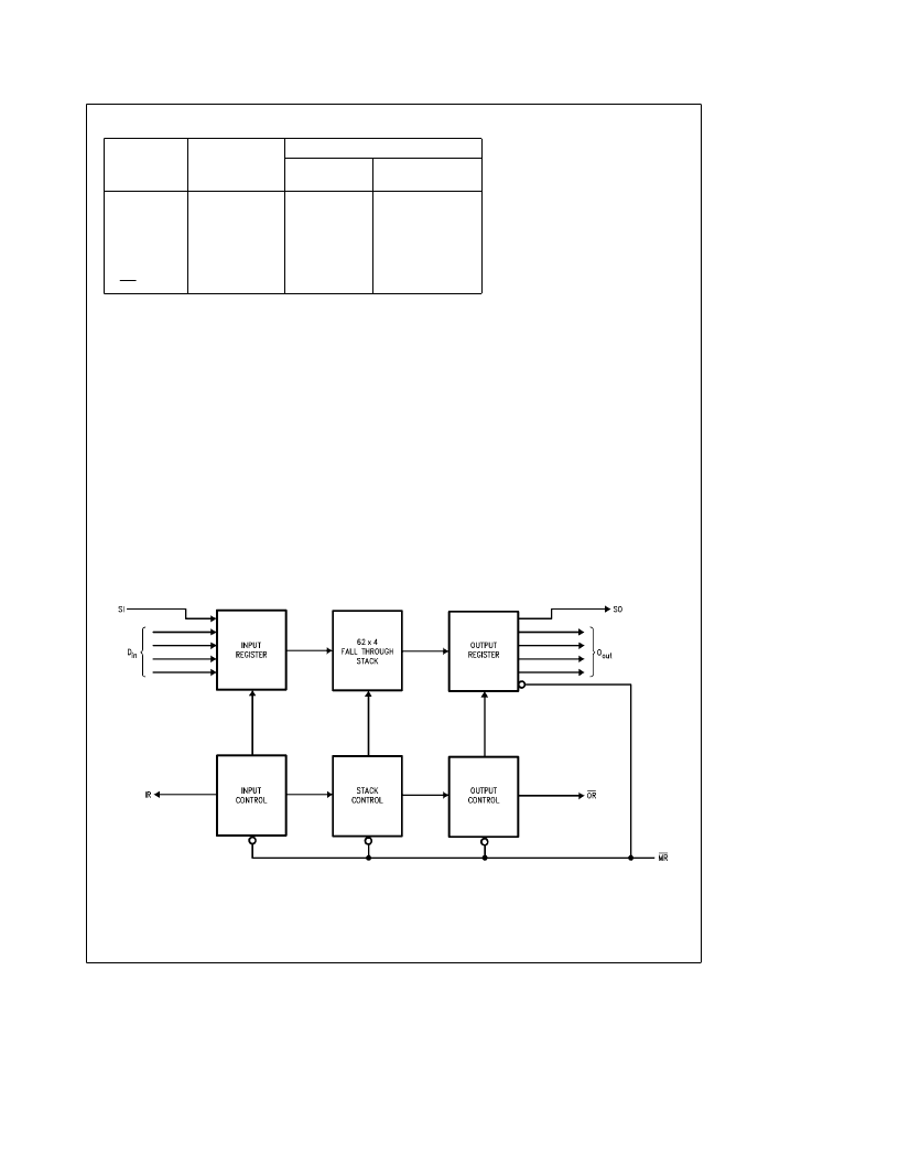
Block Diagram
TL/F/9541–4
2
相關PDF資料 |
PDF描述 |
|---|---|
| 74F521 | 8-Bit Identity Comparator(8位相同比較器) |
| 74F541 | Octal Buffer/Line Driver with TRI-STATE Outputs(三態(tài)輸出的八緩沖器/線驅動器) |
| 74F646BFCQB | Octal Transceiver/Register with TRI-STATE Outputs |
| 74F646BFCX | Octal Transceiver/Register with TRI-STATE Outputs |
| 74F646BFMQB | Octal Transceiver/Register with TRI-STATE Outputs |
相關代理商/技術參數 |
參數描述 |
|---|---|
| 74F413P-CQB | 制造商:NSC 制造商全稱:National Semiconductor 功能描述:64 x 4 First-In First-Out Buffer Memory with Parallel I/O |
| 74F413P-MQB | 制造商:NSC 制造商全稱:National Semiconductor 功能描述:64 x 4 First-In First-Out Buffer Memory with Parallel I/O |
| 74F420 WAF | 制造商:Fairchild Semiconductor Corporation 功能描述: |
| 74F433 | 制造商:FAIRCHILD 制造商全稱:Fairchild Semiconductor 功能描述:First-In First-Out (FIFO) Buffer Memory |
| 74F433 WAF | 制造商:Fairchild Semiconductor Corporation 功能描述: |
發(fā)布緊急采購,3分鐘左右您將得到回復。