- 您現(xiàn)在的位置:買賣IC網(wǎng) > PDF目錄360433 > 74F3040 (NXP Semiconductors N.V.) Dual 4-input NAND 30 ohm line driver PDF資料下載
參數(shù)資料
| 型號(hào): | 74F3040 |
| 廠商: | NXP Semiconductors N.V. |
| 英文描述: | Dual 4-input NAND 30 ohm line driver |
| 中文描述: | 雙路4輸入NAND 30歐姆的線路驅(qū)動(dòng)器 |
| 文件頁(yè)數(shù): | 4/8頁(yè) |
| 文件大?。?/td> | 71K |
| 代理商: | 74F3040 |
Philips Semiconductors
Product specification
74F3040
Dual 4-input NAND 30
line driver
1990 Jan 29
4
DC ELECTRICAL CHARACTERISTICS
(Over recommended operating free-air temperature range unless otherwise noted.)
SYMBOL
PARAMETER
TEST CONDITIONS
1
LIMITS
UNIT
MIN
TYP
2
MAX
V
CC
= MIN
V
IL
= MAX
V
IH
= MIN
= 45mA
I
OH
= –45mA
±
10% V
CC
±
5% V
CC
±
10% V
CC
2.5
V
V
OH
High-level output current
2.7
3.4
V
I
OH1
= –67mA
3
V
V
OL
Low level output current
Low-level output current
V
CC
= MIN
V
IL
= MAX
V
IH
= MIN
I
OL
= 100mA
±
10% V
CC
0.30
0.50
V
I
OL1
= 160mA
4
±
5% V
CC
0.30
0.50
V
V
IK
Input clamp voltage
V
CC
= MIN, I
I
= I
IK
–0.73
–1.2
V
I
I
Input current at maximum input
voltage
V
CC
= MAX, V
I
= 7.0V
100
μ
A
I
IH
I
IL
I
O
High-level input current
V
CC
= MAX, V
I
= 2.7V
V
CC
= MAX, V
I
= 0.5V
V
CC
= MAX, V
O
= 2.25V
20
μ
A
Low-level input current
Output current
5
–0.6
mA
–100
–200
mA
I
CC
Supply current (total)
I
CCH
I
CCL
V
CC
= MAX
3.0
5.0
mA
16
22
mA
NOTES:
1. For conditions shown as MIN or MAX, use the appropriate value specified under recommended operating conditions for the applicable type.
2. All typical values are at V
CC
= 5V, T
amb
= 25
°
C.
3. I
OH1
is the current necessary to guarantee the Low-to-High transition in a 30
transmission line on the incident wave.
4. I
OL1
is the current necessary to guarantee the High-to-Low transition in a 30
transmission line on the incident wave.
5. I
O
is tested under conditions that produce current approximately one half of the true short-circuit output current (I
OS
).
AC ELECTRICAL CHARACTERISTICS
LIMITS
SYMBOL
PARAMETER
TEST
CONDITION
T
amb
= +25
°
C
V
CC
= +5.0V
C
L
= 50pF, R
L
= 500
T
amb
= 0
°
C to +70
°
C
V
CC
= +5.0V
±
10%
C
L
= 50pF, R
L
= 500
UNIT
MIN
TYP
MAX
MIN
MAX
t
PLH
t
PHL
Propagation delay
Dna, Dnb, Dnc, Dnd to Qn
Waveform 1
1.0
1.0
2.0
2.0
5.0
4.5
1.0
1.0
5.5
5.0
ns
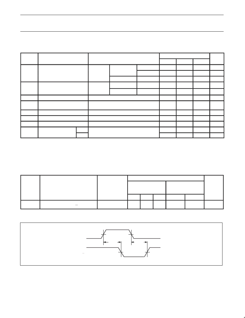
AC WAVEFORMS
For all waveforms, V
M
= 1.5V.
V
M
V
M
V
M
V
M
Qn
Dna, Dnb, Dnc, Dnd
t
PHL
t
PLH
SF00069
Waveform 1. Propagation Delay for Inputs to Output
相關(guān)PDF資料 |
PDF描述 |
|---|---|
| 74F30SCX | Single 8-input NAND Gate |
| 74F30SJX | Single 8-input NAND Gate |
| 74F30PC | 8-Input NAND Gate |
| 74F30SC | 8-Input NAND Gate |
| 74F30SJ | 8-Input NAND Gate |
相關(guān)代理商/技術(shù)參數(shù) |
參數(shù)描述 |
|---|---|
| 74F30640N | 制造商:NXP Semiconductors 功能描述:F/FAST SERIES, 8-BIT TRANSCEIVER, INVERTED OUTPUT, PDIP24 |
| 74F30D | 制造商:NXP Semiconductors 功能描述:8-BIT NAND GATE |
| 74F30N | 制造商:NXP Semiconductors 功能描述:8-BIT NAND GATE |
| 74F30PC | 功能描述:邏輯門 8-Input NAND Gate RoHS:否 制造商:Texas Instruments 產(chǎn)品:OR 邏輯系列:LVC 柵極數(shù)量:2 線路數(shù)量(輸入/輸出):2 / 1 高電平輸出電流:- 16 mA 低電平輸出電流:16 mA 傳播延遲時(shí)間:3.8 ns 電源電壓-最大:5.5 V 電源電壓-最小:1.65 V 最大工作溫度:+ 125 C 安裝風(fēng)格:SMD/SMT 封裝 / 箱體:DCU-8 封裝:Reel |
| 74F30SC | 功能描述:邏輯門 8-Input NAND Gate RoHS:否 制造商:Texas Instruments 產(chǎn)品:OR 邏輯系列:LVC 柵極數(shù)量:2 線路數(shù)量(輸入/輸出):2 / 1 高電平輸出電流:- 16 mA 低電平輸出電流:16 mA 傳播延遲時(shí)間:3.8 ns 電源電壓-最大:5.5 V 電源電壓-最小:1.65 V 最大工作溫度:+ 125 C 安裝風(fēng)格:SMD/SMT 封裝 / 箱體:DCU-8 封裝:Reel |
發(fā)布緊急采購(gòu),3分鐘左右您將得到回復(fù)。