- 您現(xiàn)在的位置:買賣IC網(wǎng) > PDF目錄360406 > 74AHCT1G02 (NXP Semiconductors N.V.) 2-input NOR gate PDF資料下載
參數(shù)資料
| 型號(hào): | 74AHCT1G02 |
| 廠商: | NXP Semiconductors N.V. |
| 英文描述: | 2-input NOR gate |
| 中文描述: | 2輸入或非門 |
| 文件頁(yè)數(shù): | 13/16頁(yè) |
| 文件大小: | 74K |
| 代理商: | 74AHCT1G02 |
第1頁(yè)第2頁(yè)第3頁(yè)第4頁(yè)第5頁(yè)第6頁(yè)第7頁(yè)第8頁(yè)第9頁(yè)第10頁(yè)第11頁(yè)第12頁(yè)當(dāng)前第13頁(yè)第14頁(yè)第15頁(yè)第16頁(yè)
2002 May 27
13
Philips Semiconductors
Product specification
2-input NAND gate
74AHC1G00; 74AHCT1G00
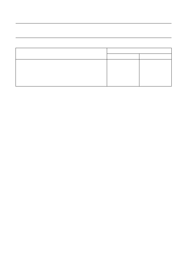
Suitability of surface mount IC packages for wave and reflow soldering methods
Notes
1.
For more detailed information on the BGA packages refer to the“(LF)BGA Application Note” (AN01026); order a copy
from your Philips Semiconductors sales office.
All surface mount (SMD) packages are moisture sensitive. Depending upon the moisture content, the maximum
temperature (with respect to time) and body size of the package, there is a risk that internal or external package
cracks may occur due to vaporization of the moisture in them (the so called popcorn effect). For details, refer to the
Drypack information in the “Data Handbook IC26; Integrated Circuit Packages; Section: Packing Methods”
These packages are not suitable for wave soldering. On versions with the heatsink on the bottom side, the solder
cannot penetrate between the printed-circuit board and the heatsink. On versions with the heatsink on the top side,
the solder might be deposited on the heatsink surface.
If wave soldering is considered, then the package must be placed at a 45
°
angle to the solder wave direction.
The package footprint must incorporate solder thieves downstream and at the side corners.
Wave soldering is suitable for LQFP, TQFP and QFP packages with a pitch (e) larger than 0.8 mm; it is definitely not
suitable for packages with a pitch (e) equal to or smaller than 0.65 mm.
Wave soldering is suitable for SSOP and TSSOP packages with a pitch (e) equal to or larger than 0.65 mm; it is
definitely not suitable for packages with a pitch (e) equal to or smaller than 0.5 mm.
2.
3.
4.
5.
6.
PACKAGE
(1)
SOLDERING METHOD
WAVE
REFLOW
(2)
BGA, LBGA, LFBGA, SQFP, TFBGA, VFBGA
HBCC, HBGA, HLQFP, HSQFP, HSOP, HTQFP, HTSSOP, HVQFN,
HVSON, SMS
PLCC
(4)
, SO, SOJ
LQFP, QFP, TQFP
SSOP, TSSOP, VSO
not suitable
not suitable
(3)
suitable
suitable
suitable
not recommended
(4)(5)
not recommended
(6)
suitable
suitable
suitable
相關(guān)PDF資料 |
PDF描述 |
|---|---|
| 74AHCT1G04 | Inverter |
| 74AHC1GU04 | Inverter |
| 74AHC1G09 | 2-input AND gate with open-drain output |
| 74AHC1G04 | Inverter |
| 74AHC1G06 | Inverter with open-drain output |
相關(guān)代理商/技術(shù)參數(shù) |
參數(shù)描述 |
|---|---|
| 74AHCT1G02DBVRE4 | 功能描述:邏輯門 Single 2-Input Positive-NOR Gate RoHS:否 制造商:Texas Instruments 產(chǎn)品:OR 邏輯系列:LVC 柵極數(shù)量:2 線路數(shù)量(輸入/輸出):2 / 1 高電平輸出電流:- 16 mA 低電平輸出電流:16 mA 傳播延遲時(shí)間:3.8 ns 電源電壓-最大:5.5 V 電源電壓-最小:1.65 V 最大工作溫度:+ 125 C 安裝風(fēng)格:SMD/SMT 封裝 / 箱體:DCU-8 封裝:Reel |
| 74AHCT1G02DBVRG4 | 功能描述:邏輯門 Single 2-Input Pos- NOR RoHS:否 制造商:Texas Instruments 產(chǎn)品:OR 邏輯系列:LVC 柵極數(shù)量:2 線路數(shù)量(輸入/輸出):2 / 1 高電平輸出電流:- 16 mA 低電平輸出電流:16 mA 傳播延遲時(shí)間:3.8 ns 電源電壓-最大:5.5 V 電源電壓-最小:1.65 V 最大工作溫度:+ 125 C 安裝風(fēng)格:SMD/SMT 封裝 / 箱體:DCU-8 封裝:Reel |
| 74AHCT1G02DBVTE4 | 功能描述:邏輯門 Single 2-Input Positive-NOR Gate RoHS:否 制造商:Texas Instruments 產(chǎn)品:OR 邏輯系列:LVC 柵極數(shù)量:2 線路數(shù)量(輸入/輸出):2 / 1 高電平輸出電流:- 16 mA 低電平輸出電流:16 mA 傳播延遲時(shí)間:3.8 ns 電源電壓-最大:5.5 V 電源電壓-最小:1.65 V 最大工作溫度:+ 125 C 安裝風(fēng)格:SMD/SMT 封裝 / 箱體:DCU-8 封裝:Reel |
| 74AHCT1G02DBVTG4 | 功能描述:邏輯門 Sgl 2-Input Pos-NAND Gate RoHS:否 制造商:Texas Instruments 產(chǎn)品:OR 邏輯系列:LVC 柵極數(shù)量:2 線路數(shù)量(輸入/輸出):2 / 1 高電平輸出電流:- 16 mA 低電平輸出電流:16 mA 傳播延遲時(shí)間:3.8 ns 電源電壓-最大:5.5 V 電源電壓-最小:1.65 V 最大工作溫度:+ 125 C 安裝風(fēng)格:SMD/SMT 封裝 / 箱體:DCU-8 封裝:Reel |
| 74AHCT1G02DCKRE4 | 功能描述:邏輯門 Single 2-Input Positive-NOR Gate RoHS:否 制造商:Texas Instruments 產(chǎn)品:OR 邏輯系列:LVC 柵極數(shù)量:2 線路數(shù)量(輸入/輸出):2 / 1 高電平輸出電流:- 16 mA 低電平輸出電流:16 mA 傳播延遲時(shí)間:3.8 ns 電源電壓-最大:5.5 V 電源電壓-最小:1.65 V 最大工作溫度:+ 125 C 安裝風(fēng)格:SMD/SMT 封裝 / 箱體:DCU-8 封裝:Reel |
發(fā)布緊急采購(gòu),3分鐘左右您將得到回復(fù)。