- 您現(xiàn)在的位置:買(mǎi)賣(mài)IC網(wǎng) > PDF目錄68811 > 71M6534-IGT/F (TERIDIAN SEMICONDUCTOR CORP) SPECIALTY ANALOG CIRCUIT, PQFP120 PDF資料下載
參數(shù)資料
| 型號(hào): | 71M6534-IGT/F |
| 廠(chǎng)商: | TERIDIAN SEMICONDUCTOR CORP |
| 元件分類(lèi): | 模擬信號(hào)調(diào)理 |
| 英文描述: | SPECIALTY ANALOG CIRCUIT, PQFP120 |
| 封裝: | LEAD FREE, LQFP-120 |
| 文件頁(yè)數(shù): | 61/124頁(yè) |
| 文件大小: | 2008K |
| 代理商: | 71M6534-IGT/F |
第1頁(yè)第2頁(yè)第3頁(yè)第4頁(yè)第5頁(yè)第6頁(yè)第7頁(yè)第8頁(yè)第9頁(yè)第10頁(yè)第11頁(yè)第12頁(yè)第13頁(yè)第14頁(yè)第15頁(yè)第16頁(yè)第17頁(yè)第18頁(yè)第19頁(yè)第20頁(yè)第21頁(yè)第22頁(yè)第23頁(yè)第24頁(yè)第25頁(yè)第26頁(yè)第27頁(yè)第28頁(yè)第29頁(yè)第30頁(yè)第31頁(yè)第32頁(yè)第33頁(yè)第34頁(yè)第35頁(yè)第36頁(yè)第37頁(yè)第38頁(yè)第39頁(yè)第40頁(yè)第41頁(yè)第42頁(yè)第43頁(yè)第44頁(yè)第45頁(yè)第46頁(yè)第47頁(yè)第48頁(yè)第49頁(yè)第50頁(yè)第51頁(yè)第52頁(yè)第53頁(yè)第54頁(yè)第55頁(yè)第56頁(yè)第57頁(yè)第58頁(yè)第59頁(yè)第60頁(yè)當(dāng)前第61頁(yè)第62頁(yè)第63頁(yè)第64頁(yè)第65頁(yè)第66頁(yè)第67頁(yè)第68頁(yè)第69頁(yè)第70頁(yè)第71頁(yè)第72頁(yè)第73頁(yè)第74頁(yè)第75頁(yè)第76頁(yè)第77頁(yè)第78頁(yè)第79頁(yè)第80頁(yè)第81頁(yè)第82頁(yè)第83頁(yè)第84頁(yè)第85頁(yè)第86頁(yè)第87頁(yè)第88頁(yè)第89頁(yè)第90頁(yè)第91頁(yè)第92頁(yè)第93頁(yè)第94頁(yè)第95頁(yè)第96頁(yè)第97頁(yè)第98頁(yè)第99頁(yè)第100頁(yè)第101頁(yè)第102頁(yè)第103頁(yè)第104頁(yè)第105頁(yè)第106頁(yè)第107頁(yè)第108頁(yè)第109頁(yè)第110頁(yè)第111頁(yè)第112頁(yè)第113頁(yè)第114頁(yè)第115頁(yè)第116頁(yè)第117頁(yè)第118頁(yè)第119頁(yè)第120頁(yè)第121頁(yè)第122頁(yè)第123頁(yè)第124頁(yè)
FDS_6533_6534_004
71M6533/71M6534 Data Sheet
v1.1
2007-2009 TERIDIAN Semiconductor Corporation
41
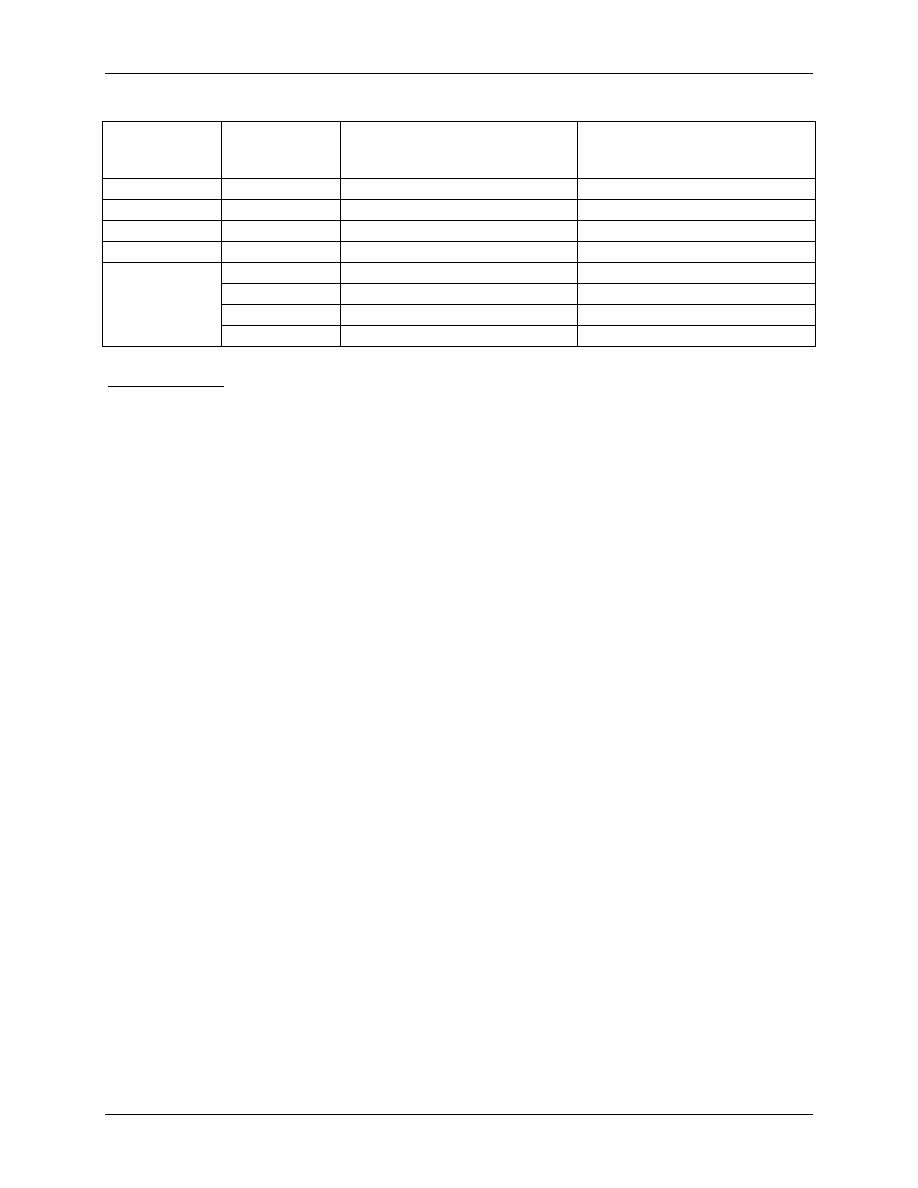
Table 38: Bank Switching with FL_BANK[2:0]
71M6533/H
71M6534
FL_BANK[1:0]
71M6534H
FL_BANK[2:0]
Address Range for Lower Bank
(0x000-0x7FFF)
Address Range for Upper Bank
(0x8000-0xFFFF)
00
000
0x0000-0x7FFF
01
001
0x0000-0x7FFF
0x8000-0xFFFF
10
010
0x0000-0x7FFF
0x10000-0x17FFF
11
011
0x0000-0x7FFF
0x18000-0x1FFFF
Not applicable
in 71M6533/H
and 71M6534
100
0x0000-0x7FFF
0x20000-0x27FFF
101
0x0000-0x7FFF
0x28000-0x2FFFF
110
0x0000-0x7FFF
0x30000-0x37FFF
111
0x0000-0x7FFF
0x38000-0x3FFFF
Program Security
When enabled, the security feature limits the ICE to global flash erase operations only. All other ICE op-
erations are blocked. This guarantees the security of the user’s MPU and CE program code. Security
should be enabled by MPU code that is executed during the pre-boot interval (60 CKMPU cycles before
the primary boot sequence begins). Once security is enabled, the only way to disable it is to perform a
global erase of the flash, followed by a chip reset.
The first 60 cycles of the MPU boot code are called the pre-boot phase because during this phase the
ICE is inhibited. A read-only status bit, PREBOOT, identifies these cycles to the MPU. Upon completion
of pre-boot, the ICE can be enabled and is permitted to take control of the MPU.
The security enable bit, SECURE, is reset whenever the chip is reset. Hardware associated with the bit
permits only ones to be written to it. Thus, pre-boot code may set SECURE to enable the security feature
but may not reset it. Once SECURE is set, the pre-boot code is protected and no external read of program
code is possible
Specifically, when SECURE is set, the following applies:
The ICE is limited to bulk flash erase only.
Page zero of flash memory, the preferred location for the user’s pre-boot code, may not be
page-erased by either MPU or ICE. Page zero may only be erased with global flash erase.
Writes to page zero, whether by MPU or ICE are inhibited.
MPU/CE RAM
The 71M6533 and 71M6534 includes 4K-bytes of static RAM memory on-chip (XRAM) plus 256 bytes of
internal RAM in the MPU core. The 4K-bytes of static RAM are used for data storage for both MPU and
CE operations.
1.4.6
UART and Optical Interface
In addition to the regular UART (UART0) the device includes an interface to implement an IR/optical port.
The pin OPT_TX is designed to directly drive an external LED for transmitting data on an optical link. The
pin OPT_RX has the same threshold as the RX pin, but can also be used to sense the input from an ex-
ternal photo detector used as the receiver for the optical link. OPT_TX and OPT_RX are connected to a
dedicated UART port (UART1).
The OPT_TX and OPT_RX pins can be inverted with configuration bits OPT_TXINV and OPT_RXINV, re-
spectively. Additionally, the OPT_TX output may be modulated at 38 kHz. Modulation is available when
system power is present (i.e. not in BROWNOUT mode). The OPT_TXMOD bit enables modulation. The duty
cycle is controlled by OPT_FDC[1:0], which can select 50%, 25%, 12.5%, and 6.25% duty cycle. A 6.25%
duty cycle means OPT_TX is low for 6.25% of the period. Figure 8 illustrates the OPT_TX generator.
相關(guān)PDF資料 |
PDF描述 |
|---|---|
| 71M6534H-IGTR/F | SPECIALTY ANALOG CIRCUIT, PQFP120 |
| 71M6533H-IGTR/F | SPECIALTY ANALOG CIRCUIT, PQFP100 |
| 71M6534-IGTR/F | SPECIALTY ANALOG CIRCUIT, PQFP120 |
| 71M6534H-IGT/F | SPECIALTY ANALOG CIRCUIT, PQFP120 |
| 71M6534-IGTR/F | SPECIALTY ANALOG CIRCUIT, PQFP120 |
相關(guān)代理商/技術(shù)參數(shù) |
參數(shù)描述 |
|---|---|
| 71M6534-IGTR/F | 功能描述:計(jì)量片上系統(tǒng) - SoC Precision Energy Meter IC RoHS:否 制造商:Maxim Integrated 核心:80515 MPU 處理器系列:71M6511 類(lèi)型:Metering SoC 最大時(shí)鐘頻率:70 Hz 程序存儲(chǔ)器大小:64 KB 數(shù)據(jù) RAM 大小:7 KB 接口類(lèi)型:UART 可編程輸入/輸出端數(shù)量:12 片上 ADC: 安裝風(fēng)格:SMD/SMT 封裝 / 箱體:LQFP-64 封裝:Reel |
| 71M6541D | 制造商:未知廠(chǎng)家 制造商全稱(chēng):未知廠(chǎng)家 功能描述:71M6541D/71M6541F/71M6541G/71M6542F/71M6542G 是 TeridianTM 的第4 代高集成度單相電表SoC |
| 71M6541D_1111 | 制造商:MAXIM 制造商全稱(chēng):Maxim Integrated Products 功能描述:Energy Meter ICs |
| 71M6541D-IGT/F | 功能描述:計(jì)量片上系統(tǒng) - SoC Precision Energy Meter IC RoHS:否 制造商:Maxim Integrated 核心:80515 MPU 處理器系列:71M6511 類(lèi)型:Metering SoC 最大時(shí)鐘頻率:70 Hz 程序存儲(chǔ)器大小:64 KB 數(shù)據(jù) RAM 大小:7 KB 接口類(lèi)型:UART 可編程輸入/輸出端數(shù)量:12 片上 ADC: 安裝風(fēng)格:SMD/SMT 封裝 / 箱體:LQFP-64 封裝:Reel |
| 71M6541D-IGTR/F | 功能描述:計(jì)量片上系統(tǒng) - SoC Precision Energy Meter IC RoHS:否 制造商:Maxim Integrated 核心:80515 MPU 處理器系列:71M6511 類(lèi)型:Metering SoC 最大時(shí)鐘頻率:70 Hz 程序存儲(chǔ)器大小:64 KB 數(shù)據(jù) RAM 大小:7 KB 接口類(lèi)型:UART 可編程輸入/輸出端數(shù)量:12 片上 ADC: 安裝風(fēng)格:SMD/SMT 封裝 / 箱體:LQFP-64 封裝:Reel |
發(fā)布緊急采購(gòu),3分鐘左右您將得到回復(fù)。