- 您現(xiàn)在的位置:買(mǎi)賣(mài)IC網(wǎng) > PDF目錄68811 > 71M6531F-IM/F (TERIDIAN SEMICONDUCTOR CORP) 1-CHANNEL POWER SUPPLY MANAGEMENT CKT, QCC68 PDF資料下載
參數(shù)資料
| 型號(hào): | 71M6531F-IM/F |
| 廠(chǎng)商: | TERIDIAN SEMICONDUCTOR CORP |
| 元件分類(lèi): | 電源管理 |
| 英文描述: | 1-CHANNEL POWER SUPPLY MANAGEMENT CKT, QCC68 |
| 封裝: | LEAD FREE, QFN-68 |
| 文件頁(yè)數(shù): | 17/120頁(yè) |
| 文件大?。?/td> | 2477K |
| 代理商: | 71M6531F-IM/F |
第1頁(yè)第2頁(yè)第3頁(yè)第4頁(yè)第5頁(yè)第6頁(yè)第7頁(yè)第8頁(yè)第9頁(yè)第10頁(yè)第11頁(yè)第12頁(yè)第13頁(yè)第14頁(yè)第15頁(yè)第16頁(yè)當(dāng)前第17頁(yè)第18頁(yè)第19頁(yè)第20頁(yè)第21頁(yè)第22頁(yè)第23頁(yè)第24頁(yè)第25頁(yè)第26頁(yè)第27頁(yè)第28頁(yè)第29頁(yè)第30頁(yè)第31頁(yè)第32頁(yè)第33頁(yè)第34頁(yè)第35頁(yè)第36頁(yè)第37頁(yè)第38頁(yè)第39頁(yè)第40頁(yè)第41頁(yè)第42頁(yè)第43頁(yè)第44頁(yè)第45頁(yè)第46頁(yè)第47頁(yè)第48頁(yè)第49頁(yè)第50頁(yè)第51頁(yè)第52頁(yè)第53頁(yè)第54頁(yè)第55頁(yè)第56頁(yè)第57頁(yè)第58頁(yè)第59頁(yè)第60頁(yè)第61頁(yè)第62頁(yè)第63頁(yè)第64頁(yè)第65頁(yè)第66頁(yè)第67頁(yè)第68頁(yè)第69頁(yè)第70頁(yè)第71頁(yè)第72頁(yè)第73頁(yè)第74頁(yè)第75頁(yè)第76頁(yè)第77頁(yè)第78頁(yè)第79頁(yè)第80頁(yè)第81頁(yè)第82頁(yè)第83頁(yè)第84頁(yè)第85頁(yè)第86頁(yè)第87頁(yè)第88頁(yè)第89頁(yè)第90頁(yè)第91頁(yè)第92頁(yè)第93頁(yè)第94頁(yè)第95頁(yè)第96頁(yè)第97頁(yè)第98頁(yè)第99頁(yè)第100頁(yè)第101頁(yè)第102頁(yè)第103頁(yè)第104頁(yè)第105頁(yè)第106頁(yè)第107頁(yè)第108頁(yè)第109頁(yè)第110頁(yè)第111頁(yè)第112頁(yè)第113頁(yè)第114頁(yè)第115頁(yè)第116頁(yè)第117頁(yè)第118頁(yè)第119頁(yè)第120頁(yè)
FDS 6531/6532 005
Data Sheet 71M6531D/F-71M6532D/F
v1.3
2005-2010 TERIDIAN Semiconductor Corporation
113
5.9
Pin Descriptions
Pin types: P = Power, O = Output, I = Input, I/O = Input/Output
The circuit number denotes the equivalent circuit, as specified under Section 5.9.4 I/O Equivalent Circuits.
5.9.1
Power and Ground Pins
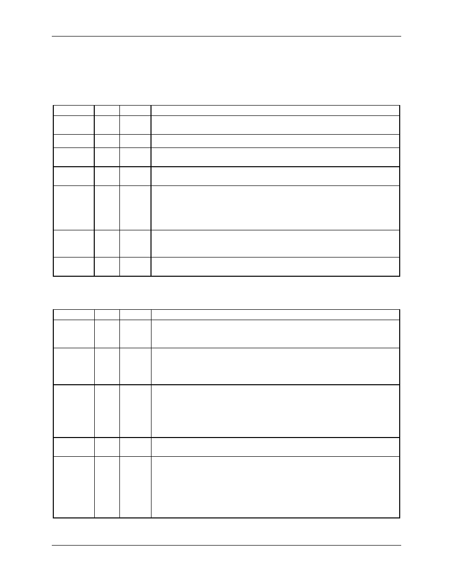
Table 90: Power and Ground Pins
Name
Type
Circuit
Description
GNDA
P
–
Analog ground: This pin should be connected directly to the ground
plane.
GNDD
P
–
Digital ground: This pin should be connected directly to the ground plane.
V3P3A
P
–
Analog power supply: A 3.3 V power supply should be connected to this
pin, must be the same voltage as V3P3SYS.
V3P3SYS
P
–
System 3.3 V supply. This pin should be connected to a 3.3 V power
supply.
V3P3D
O
13
Auxiliary voltage output of the chip, controlled by the internal 3.3 V selection
switch. In mission mode, this pin is internally connected to V3P3SYS. In
BROWNOUT mode, it is internally connected to VBAT. This pin is floating
in LCD and sleep mode. A bypass capacitor to ground should not exceed
0.1 F.
VBAT
P
12
Battery backup and oscillator power supply. A battery or super-capacitor
is to be connected between VBAT and GNDD. If no battery is used,
connect VBAT to V3P3SYS.
V2P5
O
10
Output of the internal 2.5 V regulator. A 0.1 F capacitor to GNDA
should be connected to this pin.
5.9.2
Analog Pins
Table 91: Analog Pins
Name
Type
Circuit
Description
IA, IB
IAP/IAN,
IBP/IBN
1)
I
6
Line Current Sense Inputs: These pins are voltage inputs to the internal
A/D converter. Typically, they are connected to the outputs of current
sensors. Unused pins must be tied to V3P3A.
VA, VB,
VX
1)
I
6
Line Voltage Sense Inputs: These pins are voltage inputs to the internal
A/D converter. Typically, they are connected to the outputs of resistor
dividers. Unused pins must be tied to V3P3A.
The VX pin is not supported by standard CE code.
V1
I
7
Comparator Input: This pin is a voltage input to the internal comparator.
The voltage applied to the pin is compared to the internal BIAS voltage
(1.6 V). If the input voltage is above VBIAS, the comparator output will
be high (1). If the comparator output is low, a voltage fault will occur. A
series resistor should be connected from V1 to the resistor divider to
provide hysteresis.
VREF
O
9
Voltage Reference for the ADC. Normally disabled and left unconnected.
If enabled, a 0.1 F capacitor to V3P3A should be connected to this pin.
XIN
XOUT
I
8
Crystal Inputs: A 32 kHz crystal should be connected across these pins.
Typically, a 33 pF capacitor is also connected from XIN to GNDA and a
15 pF capacitor is connected from XOUT to GNDA. It is important to
minimize the capacitance between these pins. See the crystal manufacturer
datasheet for details.
If an external clock is used, a 150 mV (p-p) clock signal should be applied
to XIN, and XOUT should be left unconnected.
1) Differential pin pairs IAP/IAN and IBP/IBN, as well as single-ended VX pin used on 71M6532D/F only.
相關(guān)PDF資料 |
PDF描述 |
|---|---|
| 71M6532D-IGTR/F | 1-CHANNEL POWER SUPPLY MANAGEMENT CKT, PQFP100 |
| 71M6531F-IM/F | 1-CHANNEL POWER SUPPLY MANAGEMENT CKT, QCC68 |
| 71M6532F-IGT/F | 1-CHANNEL POWER SUPPLY MANAGEMENT CKT, PQFP100 |
| 71M6531F-IMR/F | 1-CHANNEL POWER SUPPLY MANAGEMENT CKT, QCC68 |
| 71M6532D-IGT/F | 1-CHANNEL POWER SUPPLY MANAGEMENT CKT, PQFP100 |
相關(guān)代理商/技術(shù)參數(shù) |
參數(shù)描述 |
|---|---|
| 71M6531F-IMR/F | 功能描述:計(jì)量片上系統(tǒng) - SoC Residential Energy Meter IC RoHS:否 制造商:Maxim Integrated 核心:80515 MPU 處理器系列:71M6511 類(lèi)型:Metering SoC 最大時(shí)鐘頻率:70 Hz 程序存儲(chǔ)器大小:64 KB 數(shù)據(jù) RAM 大小:7 KB 接口類(lèi)型:UART 可編程輸入/輸出端數(shù)量:12 片上 ADC: 安裝風(fēng)格:SMD/SMT 封裝 / 箱體:LQFP-64 封裝:Reel |
| 71M6531F-IMR/F3 | 功能描述:計(jì)量片上系統(tǒng) - SoC Residential Energy Meter IC RoHS:否 制造商:Maxim Integrated 核心:80515 MPU 處理器系列:71M6511 類(lèi)型:Metering SoC 最大時(shí)鐘頻率:70 Hz 程序存儲(chǔ)器大小:64 KB 數(shù)據(jù) RAM 大小:7 KB 接口類(lèi)型:UART 可編程輸入/輸出端數(shù)量:12 片上 ADC: 安裝風(fēng)格:SMD/SMT 封裝 / 箱體:LQFP-64 封裝:Reel |
| 71M6531F-IMR/F8 | 功能描述:計(jì)量片上系統(tǒng) - SoC Residential Energy Meter IC RoHS:否 制造商:Maxim Integrated 核心:80515 MPU 處理器系列:71M6511 類(lèi)型:Metering SoC 最大時(shí)鐘頻率:70 Hz 程序存儲(chǔ)器大小:64 KB 數(shù)據(jù) RAM 大小:7 KB 接口類(lèi)型:UART 可編程輸入/輸出端數(shù)量:12 片上 ADC: 安裝風(fēng)格:SMD/SMT 封裝 / 箱體:LQFP-64 封裝:Reel |
| 71M6531F-MR/F/PE2 | 功能描述:計(jì)量片上系統(tǒng) - SoC Residential Energy Meter IC RoHS:否 制造商:Maxim Integrated 核心:80515 MPU 處理器系列:71M6511 類(lèi)型:Metering SoC 最大時(shí)鐘頻率:70 Hz 程序存儲(chǔ)器大小:64 KB 數(shù)據(jù) RAM 大小:7 KB 接口類(lèi)型:UART 可編程輸入/輸出端數(shù)量:12 片上 ADC: 安裝風(fēng)格:SMD/SMT 封裝 / 箱體:LQFP-64 封裝:Reel |
| 71M6531F-MR/F/PE3 | 功能描述:計(jì)量片上系統(tǒng) - SoC Residential Energy Meter IC RoHS:否 制造商:Maxim Integrated 核心:80515 MPU 處理器系列:71M6511 類(lèi)型:Metering SoC 最大時(shí)鐘頻率:70 Hz 程序存儲(chǔ)器大小:64 KB 數(shù)據(jù) RAM 大小:7 KB 接口類(lèi)型:UART 可編程輸入/輸出端數(shù)量:12 片上 ADC: 安裝風(fēng)格:SMD/SMT 封裝 / 箱體:LQFP-64 封裝:Reel |
發(fā)布緊急采購(gòu),3分鐘左右您將得到回復(fù)。