- 您現(xiàn)在的位置:買賣IC網(wǎng) > PDF目錄298416 > 5V2528PGI (INTEGRATED DEVICE TECHNOLOGY INC) 5V SERIES, PLL BASED CLOCK DRIVER, 10 TRUE OUTPUT(S), 0 INVERTED OUTPUT(S), PDSO28 PDF資料下載
參數(shù)資料
| 型號(hào): | 5V2528PGI |
| 廠商: | INTEGRATED DEVICE TECHNOLOGY INC |
| 元件分類: | 時(shí)鐘及定時(shí) |
| 英文描述: | 5V SERIES, PLL BASED CLOCK DRIVER, 10 TRUE OUTPUT(S), 0 INVERTED OUTPUT(S), PDSO28 |
| 封裝: | TSSOP-28 |
| 文件頁(yè)數(shù): | 2/7頁(yè) |
| 文件大小: | 333K |
| 代理商: | 5V2528PGI |
2
INDUSTRIALTEMPERATURERANGE
IDT5V2528/A
2.5 / 3.3V PHASE-LOCK LOOP CLOCK DRIVER
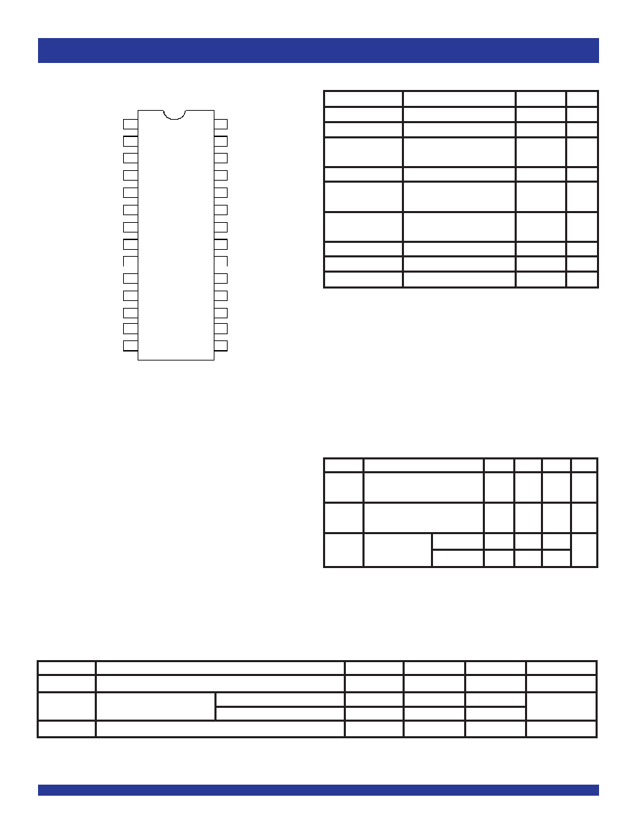
PIN CONFIGURATION
TSSOP
TOP VIEW
G_Ctrl
GND
TY1
VDDQ
TY2
GND
FBOUT
VDD
Y0
Y1
GND
TY3
VDDQ
TY6
T_Ctrl
GND
TY0
VDDQ
AVDD
CLK
FBIN
AGND
GND
TY7
28
27
26
25
24
23
22
21
20
19
1
2
3
4
5
6
7
8
9
10
TY4
VDDQ
TY5
GND
18
17
11
12
16
15
13
14
Symbol
Rating
Max.
Unit
VDD, VDDQ, AVDD
Supply Voltage Range
–0.5 to +4.6
V
VI(2)
InputVoltageRange
–0.5 to +5.5
V
VO(2)
Voltage Range applied to any
–0.5 to
V
output in the HIGH or LOW state
VDD+0.5
IIK (VI < 0)
Input Clamp Current
–50
mA
IOK
Output Clamp Current
±50
mA
(VO < 0 or VO > VDD)
IO
ContinuousOutputCurrent
±50
mA
(VO = 0 to VDD)
VDD or GND
ContinuousCurrent
±200
mA
TSTG
StorageTemperatureRange
–65 to +150
° C
TJ
JunctionTemperature
+150
° C
NOTES:
1. Stresses greater than those listed under ABSOLUTE MAXIMUM RATINGS may cause
permanent damage to the device. This is a stress rating only and functional operation
of the device at these or any other conditions above those indicated in the operational
sections of this specification is not implied. Exposure to absolute maximum rating
conditions for extended periods may affect reliability.
2. The input and output negative-voltage ratings may be exceeded if the input and output
clamp-current ratings are observed.
3. The maximum package power dissipation is calculated using a junction temperature
of 150
°C and a board trace length of 750 mils.
ABSOLUTE MAXIMUM RATINGS(1)
Symbol
Description
Min.
Typ.
Max.
Unit
VDD, AVDD (1)
Power Supply Voltage
3
3.3
3.6
V
VDDQ(1)
Power Supply Voltage
2.5V Outputs
2.3
2.5
2.7
V
3.3V Outputs
3
3.3
3.6
TA
AmbientOperatingTemperature
–40
+25
+85
° C
RECOMMENDED OPERATING RANGE
Symbol
Description
Min
Typ.
Max.
Unit
CIN
Input Capacitance
—
5
—
pF
VI = VDD or GND
CO
Output Capacitance
—
6
—
pF
VI = VDD or GND
CL
Load Capacitance
2.5V outputs
—
20
—
pF
3.3V outputs
—
30
—
CAPACITANCE(1)
NOTE:
1. Unused inputs must be held HIGH or LOW to prevent them from floating.
NOTE:
1. All power supplies should operate in tandem. If VDD or VDDQ is at a maximum, then VDDQ or VDD (respectively) should be at maximum, and vice-versa.
相關(guān)PDF資料 |
PDF描述 |
|---|---|
| 6-104186-5 | 30 CONTACT(S), MALE, RIGHT ANGLE TWO PART BOARD CONNECTOR, SOLDER |
| 6-1394461-1 | Solar Connector Cable Coupler |
| 6-1394461-2 | Solar Connector Cable Coupler |
| 6-1394461-4 | Solar Connector Cable Coupler |
| 6-1394461-5 | Solar Connector Cable Coupler |
相關(guān)代理商/技術(shù)參數(shù) |
參數(shù)描述 |
|---|---|
| 5V2A-21-NEG-WALL | 制造商:Gravitech 功能描述:Plug-In AC Adapters 5V 1A 2.1MM POSITIVE CENTER WALL ADAPTER |
| 5V2A-21-POS-WALL | 制造商:Gravitech 功能描述:Plug-In AC Adapters 5V 1A 2.1MM POSITIVE CENTER WALL ADAPTER |
| 5V2WH43TP4 | 制造商:C&K Components 功能描述: 制造商:undefined 功能描述: |
| 5V30022DCG | 功能描述:時(shí)鐘緩沖器 2.5V ZD CLK BUFFER SS RoHS:否 制造商:Texas Instruments 輸出端數(shù)量:5 最大輸入頻率:40 MHz 傳播延遲(最大值): 電源電壓-最大:3.45 V 電源電壓-最小:2.375 V 最大功率耗散: 最大工作溫度:+ 85 C 最小工作溫度:- 40 C 封裝 / 箱體:LLP-24 封裝:Reel |
| 5V30022DCG8 | 功能描述:時(shí)鐘緩沖器 2.5V ZD CLK BUFFER SS RoHS:否 制造商:Texas Instruments 輸出端數(shù)量:5 最大輸入頻率:40 MHz 傳播延遲(最大值): 電源電壓-最大:3.45 V 電源電壓-最小:2.375 V 最大功率耗散: 最大工作溫度:+ 85 C 最小工作溫度:- 40 C 封裝 / 箱體:LLP-24 封裝:Reel |
發(fā)布緊急采購(gòu),3分鐘左右您將得到回復(fù)。