- 您現(xiàn)在的位置:買(mǎi)賣(mài)IC網(wǎng) > PDF目錄233104 > 5T9310NLGI (INTEGRATED DEVICE TECHNOLOGY INC) 5T SERIES, LOW SKEW CLOCK DRIVER, 10 TRUE OUTPUT(S), 0 INVERTED OUTPUT(S), PQCC40 PDF資料下載
參數(shù)資料
| 型號(hào): | 5T9310NLGI |
| 廠商: | INTEGRATED DEVICE TECHNOLOGY INC |
| 元件分類(lèi): | 時(shí)鐘及定時(shí) |
| 英文描述: | 5T SERIES, LOW SKEW CLOCK DRIVER, 10 TRUE OUTPUT(S), 0 INVERTED OUTPUT(S), PQCC40 |
| 封裝: | PLASTIC, QFN-40 |
| 文件頁(yè)數(shù): | 10/13頁(yè) |
| 文件大小: | 225K |
| 代理商: | 5T9310NLGI |
第1頁(yè)第2頁(yè)第3頁(yè)第4頁(yè)第5頁(yè)第6頁(yè)第7頁(yè)第8頁(yè)第9頁(yè)當(dāng)前第10頁(yè)第11頁(yè)第12頁(yè)第13頁(yè)
INDUSTRIALTEMPERATURERANGE
6
IDT5T9310
2.5VLVDS1:10CLOCKBUFFERTERABUFFERII
DIFFERENTIAL INPUT AC TEST CONDITIONS FOR LVDS
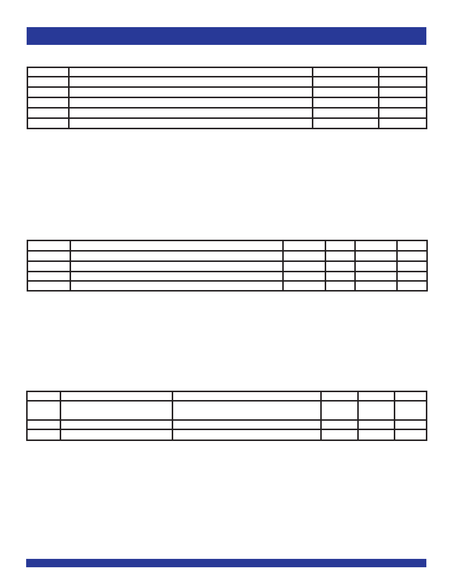
Symbol
Parameter
Value
Units
VDIF
Input Signal Swing(1)
400
mV
VX
DifferentialInputSignalCrossingPoint(2)
1.2
V
DH
Duty Cycle
50
%
VTHI
InputTimingMeasurementReferenceLevel(3)
CrossingPoint
V
tR, tF
InputSignalEdgeRate(4)
2
V/ns
NOTES:
1. The 400mV peak-to-peak input pulse level is specified to allow consistent, repeatable results in an automatic test equipment (ATE) environment. This device meets the VDIF (AC)
specification under actual use conditions.
2. A 1.2V crossing point level is specified to allow consistent, repeatable results in an automatic test equipment (ATE) environment. This device meets the VX specification under
actual use conditions.
3. In all cases, input waveform timing is marked at the differential cross-point of the input signals.
4. The input signal edge rate of 2V/ns or greater is to be maintained in the 20% to 80% range of the input waveform.
POWER SUPPLY CHARACTERISTICS FOR LVDS OUTPUTS(1)
Symbol
Parameter
Test Conditions
Typ.
Max
Unit
IDDQ
Quiescent VDD Power Supply Current
VDD = Max., All Input Clocks = LOW(2)
—
295
mA
Outputsenabled
ITOT
Total Power VDD Supply Current
VDD = 2.7V., FREFERENCE CLOCK = 1GHz
—
305
mA
IPD
Total Power Down Supply Current
PD = LOW
—
5
mA
NOTES:
1. These power consumption characteristics are for all the valid input interfaces and cover the worst case conditions.
2. The true input is held LOW and the complementary input is held HIGH.
AC DIFFERENTIAL INPUT SPECIFICATIONS(1)
Symbol
Parameter
Min.
Typ.
Max
Unit
VDIF
ACDifferentialVoltage(2)
0.1
—
3.6
V
VIX
DifferentialInputCrosspointVoltage
0.05
—
VDD
V
VCM
CommonModeInputVoltageRange(3)
0.05
—
VDD
V
VIN
InputVoltage
- 0.3
+3.6
V
NOTES:
1. The output will not change state until the inputs have crossed and the minimum differential voltage range defined by VDIF has been met or exceeded.
2. VDIF specifies the minimum input voltage (VTR - VCP) required for switching where VTR is the "true" input level and VCP is the "complement" input level. The AC differential voltage
must be achieved to guarantee switching to a new state.
3. VCM specifies the maximum allowable range of (VTR + VCP) /2.
相關(guān)PDF資料 |
PDF描述 |
|---|---|
| 54HHSC163CE | HSC SERIES, SYN POSITIVE EDGE TRIGGERED 4-BIT UP BINARY COUNTER, CDIP16 |
| 54HSC154LS | HSC SERIES, OTHER DECODER/DRIVER, INVERTED OUTPUT, CQCC28 |
| 54RHST139CD | HST/T SERIES, OTHER DECODER/DRIVER, INVERTED OUTPUT, CDIP16 |
| 54QHST253LD | HST/T SERIES, DUAL 4 LINE TO 1 LINE MULTIPLEXER, TRUE OUTPUT, CQCC20 |
| 54QHST253LE | HST/T SERIES, DUAL 4 LINE TO 1 LINE MULTIPLEXER, TRUE OUTPUT, CQCC20 |
相關(guān)代理商/技術(shù)參數(shù) |
參數(shù)描述 |
|---|---|
| 5T9310NLGI8 | 功能描述:時(shí)鐘驅(qū)動(dòng)器及分配 2.5V LVDS 1:10 Clock Buffer RoHS:否 制造商:Micrel 乘法/除法因子:1:4 輸出類(lèi)型:Differential 最大輸出頻率:4.2 GHz 電源電壓-最大: 電源電壓-最小:5 V 最大工作溫度:+ 85 C 封裝 / 箱體:SOIC-8 封裝:Reel |
| 5T9310NLI | 制造商:Integrated Device Technology Inc 功能描述:Clock Driver 2-IN LVDS 40-Pin VFQFPN EP Tray 制造商:IDT 功能描述:Clock Driver 2-IN LVDS 40-Pin VFQFPN EP Tray |
| 5T9310-NLI | 制造商:Integrated Device Technology Inc 功能描述:Clock Driver 2-IN LVDS 40-Pin VFQFPN EP Tray 制造商:IDT 功能描述:Clock Driver 2-IN LVDS 40-Pin VFQFPN EP Tray |
| 5T9316NLGI | 功能描述:時(shí)鐘緩沖器 TeraBuffer II 2.5V LVDS 1:16 Clk Buffer RoHS:否 制造商:Texas Instruments 輸出端數(shù)量:5 最大輸入頻率:40 MHz 傳播延遲(最大值): 電源電壓-最大:3.45 V 電源電壓-最小:2.375 V 最大功率耗散: 最大工作溫度:+ 85 C 最小工作溫度:- 40 C 封裝 / 箱體:LLP-24 封裝:Reel |
| 5T9316NLGI8 | 功能描述:時(shí)鐘驅(qū)動(dòng)器及分配 TeraBuffer II 2.5V LVDS 1:16 Clk Buffer RoHS:否 制造商:Micrel 乘法/除法因子:1:4 輸出類(lèi)型:Differential 最大輸出頻率:4.2 GHz 電源電壓-最大: 電源電壓-最小:5 V 最大工作溫度:+ 85 C 封裝 / 箱體:SOIC-8 封裝:Reel |
發(fā)布緊急采購(gòu),3分鐘左右您將得到回復(fù)。